- 您現(xiàn)在的位置:買(mǎi)賣(mài)IC網(wǎng) > PDF目錄4139 > XCS40XL-5PQ208C (Xilinx Inc)IC FPGA 3.3V C-TEMP 208-PQFP PDF資料下載
參數(shù)資料
| 型號(hào): | XCS40XL-5PQ208C |
| 廠商: | Xilinx Inc |
| 文件頁(yè)數(shù): | 61/83頁(yè) |
| 文件大?。?/td> | 0K |
| 描述: | IC FPGA 3.3V C-TEMP 208-PQFP |
| 產(chǎn)品變化通告: | Product Discontinuation 26/Oct/2011 |
| 標(biāo)準(zhǔn)包裝: | 24 |
| 系列: | Spartan®-XL |
| LAB/CLB數(shù): | 784 |
| 邏輯元件/單元數(shù): | 1862 |
| RAM 位總計(jì): | 25088 |
| 輸入/輸出數(shù): | 169 |
| 門(mén)數(shù): | 40000 |
| 電源電壓: | 3 V ~ 3.6 V |
| 安裝類(lèi)型: | 表面貼裝 |
| 工作溫度: | 0°C ~ 85°C |
| 封裝/外殼: | 208-BFQFP |
| 供應(yīng)商設(shè)備封裝: | 208-PQFP(28x28) |
第1頁(yè)第2頁(yè)第3頁(yè)第4頁(yè)第5頁(yè)第6頁(yè)第7頁(yè)第8頁(yè)第9頁(yè)第10頁(yè)第11頁(yè)第12頁(yè)第13頁(yè)第14頁(yè)第15頁(yè)第16頁(yè)第17頁(yè)第18頁(yè)第19頁(yè)第20頁(yè)第21頁(yè)第22頁(yè)第23頁(yè)第24頁(yè)第25頁(yè)第26頁(yè)第27頁(yè)第28頁(yè)第29頁(yè)第30頁(yè)第31頁(yè)第32頁(yè)第33頁(yè)第34頁(yè)第35頁(yè)第36頁(yè)第37頁(yè)第38頁(yè)第39頁(yè)第40頁(yè)第41頁(yè)第42頁(yè)第43頁(yè)第44頁(yè)第45頁(yè)第46頁(yè)第47頁(yè)第48頁(yè)第49頁(yè)第50頁(yè)第51頁(yè)第52頁(yè)第53頁(yè)第54頁(yè)第55頁(yè)第56頁(yè)第57頁(yè)第58頁(yè)第59頁(yè)第60頁(yè)當(dāng)前第61頁(yè)第62頁(yè)第63頁(yè)第64頁(yè)第65頁(yè)第66頁(yè)第67頁(yè)第68頁(yè)第69頁(yè)第70頁(yè)第71頁(yè)第72頁(yè)第73頁(yè)第74頁(yè)第75頁(yè)第76頁(yè)第77頁(yè)第78頁(yè)第79頁(yè)第80頁(yè)第81頁(yè)第82頁(yè)第83頁(yè)
Spartan and Spartan-XL FPGA Families Data Sheet
64
DS060 (v2.0) March 1, 2013
Product Specification
R
Product Obsolete/Under Obsolescence
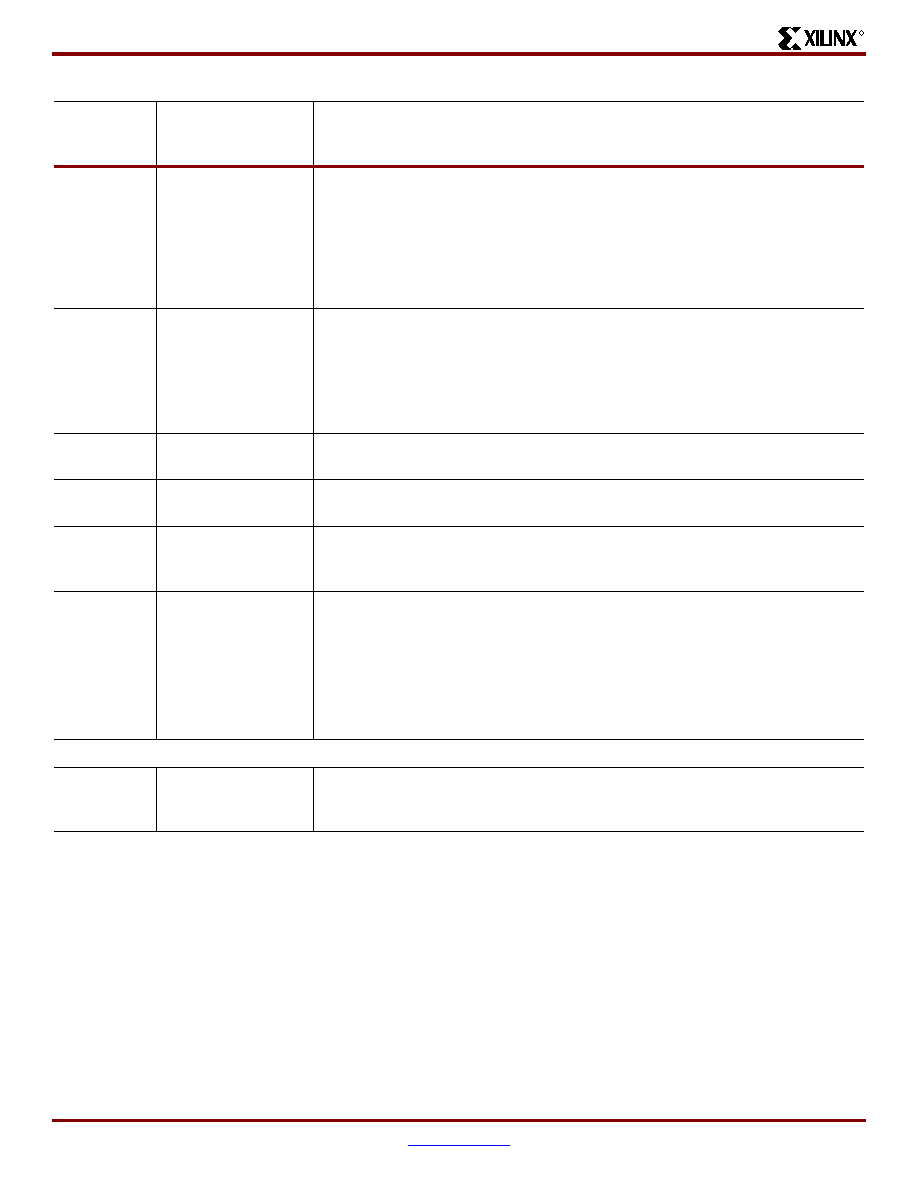
SGCK1 -
SGCK4
(Spartan)
Weak
Pull-up
(except
SGCK4
is DOUT)
I or I/O
Four Secondary Global inputs each drive a dedicated internal global net with short
delay and minimal skew. These internal global nets can also be driven from
internal logic. If not used to drive a global net, any of these pins is a
user-programmable I/O pin.
The SGCK1-SGCK4 pins provide the shortest path to the four Secondary Global
Buffers. Any input pad symbol connected directly to the input of a BUFGS symbol
is automatically placed on one of these pins.
GCK1 -
GCK8
(Spartan-XL)
Weak
Pull-up
(except
GCK6 is
DOUT)
I or I/O
Eight Global inputs each drive a dedicated internal global net with short delay and
minimal skew. These internal global nets can also be driven from internal logic. If
not used to drive a global net, any of these pins is a user-programmable I/O pin.
The GCK1-GCK8 pins provide the shortest path to the eight Global Low-Skew
Buffers. Any input pad symbol connected directly to the input of a BUFGLS symbol
is automatically placed on one of these pins.
CS1
(Spartan-XL)
I
I/O
During Express configuration, CS1 is used as a serial-enable signal for
daisy-chaining.
D0-D7
(Spartan-XL)
I
I/O
During Express configuration, these eight input pins receive configuration data.
After configuration, they are user-programmable I/O pins.
DIN
I
I/O
During Slave Serial or Master Serial configuration, DIN is the serial configuration
data input receiving data on the rising edge of CCLK. After configuration, DIN is a
user-programmable I/O pin.
DOUT
O
I/O
During Slave Serial or Master Serial configuration, DOUT is the serial
configuration data output that can drive the DIN of daisy-chained slave FPGAs.
DOUT data changes on the falling edge of CCLK, one-and-a-half CCLK periods
after it was received at the DIN input.
In Spartan-XL family Express mode, DOUT is the status output that can drive the
CS1 of daisy-chained FPGAs, to enable and disable downstream devices.
After configuration, DOUT is a user-programmable I/O pin.
Unrestricted User-Programmable I/O Pins
I/O
Weak
Pull-up
I/O
These pins can be configured to be input and/or output after configuration is
completed. Before configuration is completed, these pins have an internal
high-value pull-up resistor network that defines the logic level as High.
Table 18: Pin Descriptions (Continued)
Pin Name
I/O
During
Config.
I/O After
Config.
Pin Description
相關(guān)PDF資料 |
PDF描述 |
|---|---|
| IDT71V35761S166BG | IC SRAM 4MBIT 166MHZ 119BGA |
| IDT71V3556SA166BG | IC SRAM 4MBIT 166MHZ 119BGA |
| IDT71V25761S200BG | IC SRAM 4MBIT 200MHZ 119BGA |
| IDT71V25761S183BG | IC SRAM 4MBIT 183MHZ 119BGA |
| IDT71V25761S166BG | IC SRAM 4MBIT 166MHZ 119BGA |
相關(guān)代理商/技術(shù)參數(shù) |
參數(shù)描述 |
|---|---|
| XCS40XL-5PQ208I | 制造商:XILINX 制造商全稱(chēng):XILINX 功能描述:Spartan and Spartan-XL FPGA |
| XCS40XL-5PQ240C | 功能描述:IC FPGA 3.3V C-TEMP 240-PQFP RoHS:否 類(lèi)別:集成電路 (IC) >> 嵌入式 - FPGA(現(xiàn)場(chǎng)可編程門(mén)陣列) 系列:Spartan®-XL 標(biāo)準(zhǔn)包裝:1 系列:Kintex-7 LAB/CLB數(shù):25475 邏輯元件/單元數(shù):326080 RAM 位總計(jì):16404480 輸入/輸出數(shù):350 門(mén)數(shù):- 電源電壓:0.97 V ~ 1.03 V 安裝類(lèi)型:表面貼裝 工作溫度:0°C ~ 85°C 封裝/外殼:900-BBGA,F(xiàn)CBGA 供應(yīng)商設(shè)備封裝:900-FCBGA(31x31) 其它名稱(chēng):122-1789 |
| XCS40XL-5PQ240I | 制造商:XILINX 制造商全稱(chēng):XILINX 功能描述:Spartan and Spartan-XL FPGA |
| XCS40XL-5PQ256C | 制造商:XILINX 制造商全稱(chēng):XILINX 功能描述:Spartan and Spartan-XL Families Field Programmable Gate Arrays |
| XCS40XL-5PQ256I | 制造商:XILINX 制造商全稱(chēng):XILINX 功能描述:Spartan and Spartan-XL Families Field Programmable Gate Arrays |
發(fā)布緊急采購(gòu),3分鐘左右您將得到回復(fù)。