- 您現(xiàn)在的位置:買賣IC網(wǎng) > PDF目錄385955 > XP1028-BD (Mimix Broadband, Inc.) 43.5-46.5 GHz GaAs MMIC Power Amplifier PDF資料下載
參數(shù)資料
| 型號(hào): | XP1028-BD |
| 廠商: | Mimix Broadband, Inc. |
| 英文描述: | 43.5-46.5 GHz GaAs MMIC Power Amplifier |
| 中文描述: | 43.5-46.5 GHz的砷化鎵單片功率放大器 |
| 文件頁(yè)數(shù): | 3/5頁(yè) |
| 文件大小: | 356K |
| 代理商: | XP1028-BD |
Page 3 of 5
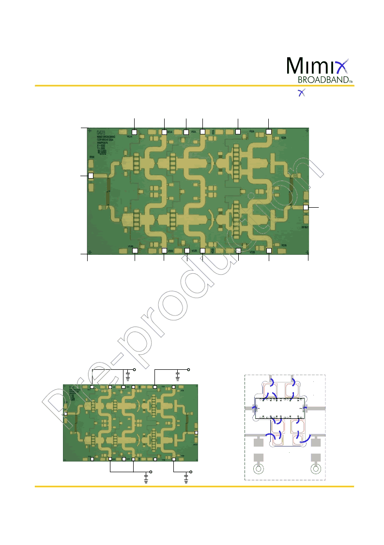
Mechanical Drawing
Bias Arrangement
43.5-46.5 GHz GaAs MMIC
Power Amplifier
Mimix Broadband, Inc., 10795 Rockley Rd., Houston, Texas 77099
Tel: 281.988.4600 Fax: 281.988.4615 mimixbroadband.com
Characteristic Data and Specifications are subject to change without notice.
2007 Mimix Broadband, Inc.
Export of this item may require appropriate export licensing from the U.S. Government. In purchasing these parts, U.S. Domestic customers accept
their obligation to be compliant with U.S. Export Laws.
April 2007 - Rev 17-Apr-07
P1028-BD
1
2
3
4
5
6
7
8
9
10
11
12
13
14
Vg1,2
RF In
RF Out
Vg3
Vd3
Vd1,2
2.490
(0.098)
1
2
3
4
5
6
7
8
9
10
11
12
13
0.937
(0.037)
1.438
(0.057)
1.937
(0.076)
2.337
(0.092)
3.538
(0.139)
2.936
(0.116)
2.337
(0.092)
1.937
(0.076)
1.438
(0.057)
0.937
(0.037)
0.0
0.0
1.549
(0.061)
14
2.936
(0.116)
3.538
(0.139)
0.933
(0.037)
4.330
(0.170)
Bypass Capacitors
- See App Note [2]
Vg1,2
Vg3
(Note: Engineering designator is 44MPA0478)
Units: millimeters (inches) Bond pad dimensions are shown to center of bond pad.
Thickness: 0.110 +/- 0.010 (0.0043 +/- 0.0004), Backside is ground, Bond Pad/Backside Metallization: Gold
All DC Bond Pads are 0.100 x 0.100 (0.004 x 0.004). All RF Bond Pads are 0.100 x 0.200 (0.004 x 0.008)
Bond pad centers are approximately 0.109 (0.004) from the edge of the chip.
Dicing tolerance: +/- 0.005 (+/- 0.0002). Approximate weight: 6.680 mg.
Bond Pad #1 (RF In)
Bond Pad #2 (Vg1A)
Bond Pad #3 (Vd1A)
Bond Pad #4 (Vg2A)
Bond Pad #5 (Vd2A)
Bond Pad #6 (Vg3A)
Bond Pad #7 (Vd3A)
Bond Pad #8 (RF Out)
Bond Pad #9 (Vd3B)
Bond Pad #10 (Vg3B)
Bond Pad #11 Vd2B)
Bond Pad #12 (Vg2B)
Bond Pad #13 (Vd1B)
Bond Pad #14 (Vg1B)
RF Out
Vd3
Vd1,2
RF In
XP1028-BD
XP1028-BD
XP1028-BD
相關(guān)PDF資料 |
PDF描述 |
|---|---|
| XP1028-BD-000V | 43.5-46.5 GHz GaAs MMIC Power Amplifier |
| XP1028-BD-EV1 | 43.5-46.5 GHz GaAs MMIC Power Amplifier |
| XP131A1715SR | N-Channel Power MOS FET |
| XP132A0340SR | P-Channel Power MOS FET |
| XP133A0245SR | N-Channel Power MOS FET |
相關(guān)代理商/技術(shù)參數(shù) |
參數(shù)描述 |
|---|---|
| XP1028-BD-000V | 制造商:MIMIX 制造商全稱:MIMIX 功能描述:43.5-46.5 GHz GaAs MMIC Power Amplifier |
| XP1028-BD-EV1 | 制造商:MIMIX 制造商全稱:MIMIX 功能描述:43.5-46.5 GHz GaAs MMIC Power Amplifier |
| XP1031-BD | 制造商:MIMIX 制造商全稱:MIMIX 功能描述:37.0-42.0 GHz GaAs MMIC Power Amplifier |
| XP1031-QK | 制造商:MIMIX 制造商全稱:MIMIX 功能描述:37.0-40.0 GHz GaAs Power Amplifier |
| XP1031-QK_09 | 制造商:MIMIX 制造商全稱:MIMIX 功能描述:37.0-40.0 GHz GaAs Power Amplifier |
發(fā)布緊急采購(gòu),3分鐘左右您將得到回復(fù)。