- 您現在的位置:買賣IC網 > PDF目錄372927 > XQ4005E-4PG156M Field Programmable Gate Array (FPGA) PDF資料下載
參數資料
| 型號: | XQ4005E-4PG156M |
| 英文描述: | Field Programmable Gate Array (FPGA) |
| 中文描述: | 現場可編程門陣列(FPGA) |
| 文件頁數: | 14/36頁 |
| 文件大小: | 304K |
| 代理商: | XQ4005E-4PG156M |
第1頁第2頁第3頁第4頁第5頁第6頁第7頁第8頁第9頁第10頁第11頁第12頁第13頁當前第14頁第15頁第16頁第17頁第18頁第19頁第20頁第21頁第22頁第23頁第24頁第25頁第26頁第27頁第28頁第29頁第30頁第31頁第32頁第33頁第34頁第35頁第36頁
R
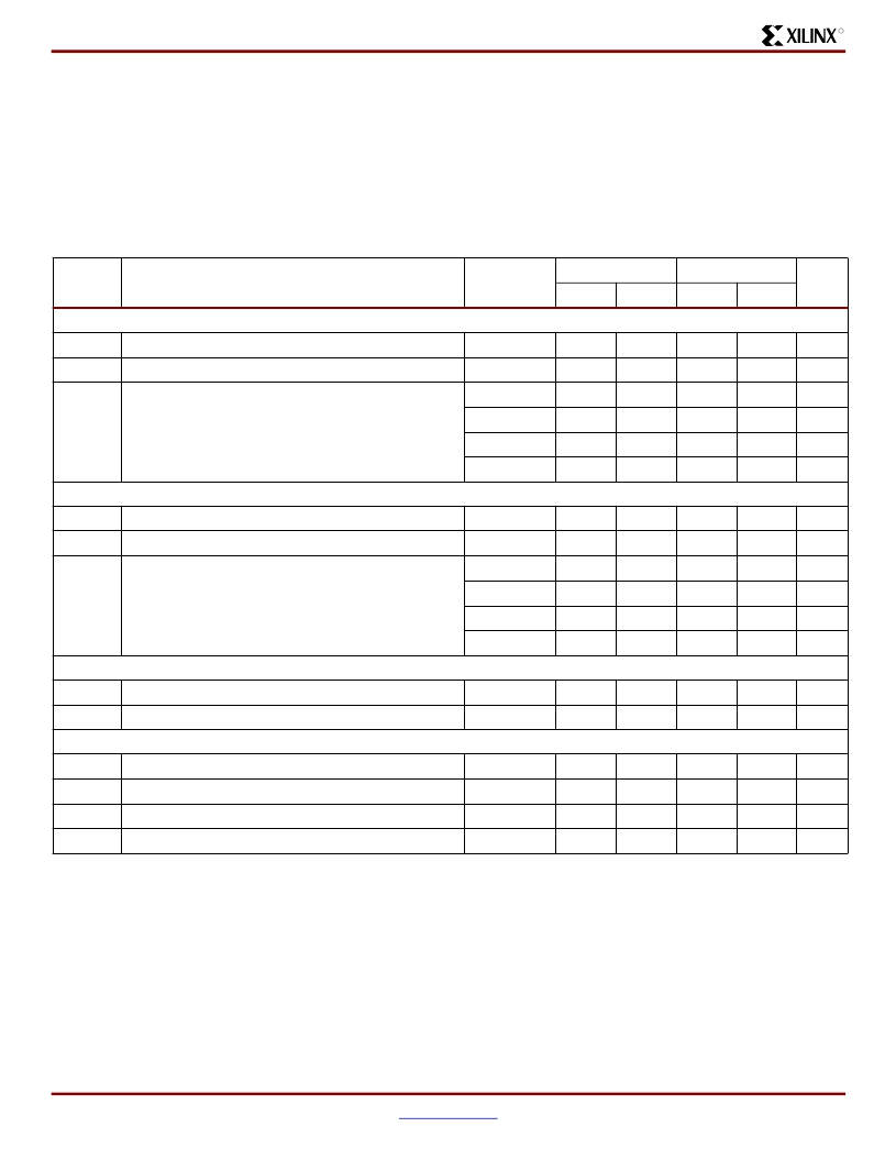
XQ4000E IOB Input Switching Characteristic Guidelines
Testing of switching parameters is modeled after testing
methods specified by MIL-M-38510/605. All devices are
100% functionally tested. Pin-to-pin timing parameters are
derived from measuring external and internal test patterns
and are guaranteed over worst-case operating conditions
(supply voltage and junction temperature). Listed below are
representative values for typical pin locations and normal
clock loading. For more specific, more precise, and
worst-case guaranteed data, reflecting the actual routing
structure, use the values provided by the static timing ana-
lyzer (TRCE in the Xilinx Development System) and
back-annotated to the simulation netlist. These path delays,
provided as a guideline, have been extracted from the static
timing analyzer report. Values apply to all XQ4000E devices
unless otherwise noted.
Symbol
Propagation Delays (TTL Inputs)
(1)
Description
Device
-3
-4
Units
Min
Max
Min
Max
T
PID
T
PLI
T
PDLI
Pad to I1, I2
All devices
-
2.5
-
3.0
ns
Pad to I1, I2 via transparent input latch, no delay
All devices
-
3.6
-
4.8
ns
Pad to I1, I2 via transparent FCL and input latch,
with delay
XQ4005E
-
-
-
10.8
ns
XQ4010E
-
10.8
-
11.0
ns
XQ4013E
-
11.2
-
11.4
ns
XQ4025E
-
-
-
13.8
ns
Propagation Delays (CMOS Inputs)
(1)
T
PIDC
T
PLIC
T
PDLIC
Pad to I1, I2
All devices
-
4.1
-
5.5
ns
Pad to I1, I2 via transparent input latch, no delay
All devices
-
8.8
-
6.8
ns
Pad to I1, I2 via transparent FCL and input latch,
with delay
XQ4005E
-
-
-
16.5
ns
XQ4010E
-
14.0
-
17.5
ns
XQ4013E
-
14.4
-
18.0
ns
XQ4025E
-
-
-
20.8
ns
Propagation Delays (TTL Inputs)
T
IKRI
T
IKLI
Hold Times
(2)
Clock (IK) to I1, I2 (flip-flop)
All devices
-
2.8
-
5.6
ns
Clock (IK) to I1, I2 (latch enable, active Low)
All devices
-
4.0
-
6.2
ns
T
IKPI
T
IKPID
T
IKEC
T
IKECD
Notes:
1.
Input pad setup and hold times are specified with respect to the internal clock (IK). For setup and hold times with respect to the clock
input pin, see the pin-to-pin parameters in the Guaranteed Input and Output Parameters table.
2.
Voltage levels of unused pads, bonded or unbonded, must be valid logic levels. Each can be configured with the internal pull-up
(default) or pull-down resistor, or configured as a driven output, or can be driven from an external source.
Pad to clock (IK), no delay
All devices
0
-
0
-
ns
Pad to clock (IK), with delay
All devices
0
-
0
-
ns
Clock enable (EC) to clock (K), no delay
All devices
1.5
-
1.5
-
ns
Clock enable (EC) to clock (K), with delay
All devices
0
-
0
-
ns
相關PDF資料 |
PDF描述 |
|---|---|
| XQ4000ESERIES | QPRO XQ4000E/EX QML High-Reliability FPGAs |
| XQ4000EXSERIES | QPRO XQ4000E/EX QML High-Reliability FPGAs |
| XQ4005E-4CB164M | Field Programmable Gate Array (FPGA) |
| XQ4005E-4HQ191N | QPRO XQ4000E/EX QML High-Reliability FPGAs |
| XQ4005E-4PG191M | QPRO XQ4000E/EX QML High-Reliability FPGAs |
相關代理商/技術參數 |
參數描述 |
|---|---|
| XQ4005E-4PG191M | 制造商:XILINX 制造商全稱:XILINX 功能描述:QML High-Reliability FPGAs |
| XQ4005E-4PG191N | 制造商:XILINX 制造商全稱:XILINX 功能描述:QML High-Reliability FPGAs |
| XQ4005E-4PG196M | 制造商:XILINX 制造商全稱:XILINX 功能描述:QML High-Reliability FPGAs |
| XQ4005E-4PG196N | 制造商:XILINX 制造商全稱:XILINX 功能描述:QML High-Reliability FPGAs |
| XQ4005EX-3BG191M | 制造商:XILINX 制造商全稱:XILINX 功能描述:QML High-Reliability FPGAs |
發(fā)布緊急采購,3分鐘左右您將得到回復。