- 您現(xiàn)在的位置:買賣IC網(wǎng) > PDF目錄372927 > XQ4005E-4PG191M (Xilinx, Inc.) QPRO XQ4000E/EX QML High-Reliability FPGAs PDF資料下載
參數(shù)資料
| 型號: | XQ4005E-4PG191M |
| 廠商: | Xilinx, Inc. |
| 元件分類: | FPGA |
| 英文描述: | QPRO XQ4000E/EX QML High-Reliability FPGAs |
| 中文描述: | QPRO XQ4000E/EX QML第高可靠性的FPGA |
| 文件頁數(shù): | 11/36頁 |
| 文件大小: | 304K |
| 代理商: | XQ4005E-4PG191M |
第1頁第2頁第3頁第4頁第5頁第6頁第7頁第8頁第9頁第10頁當(dāng)前第11頁第12頁第13頁第14頁第15頁第16頁第17頁第18頁第19頁第20頁第21頁第22頁第23頁第24頁第25頁第26頁第27頁第28頁第29頁第30頁第31頁第32頁第33頁第34頁第35頁第36頁
QPRO XQ4000E/EX QML High-Reliability FPGAs
DS021 (v2.2) June 25, 2000
Product Specification
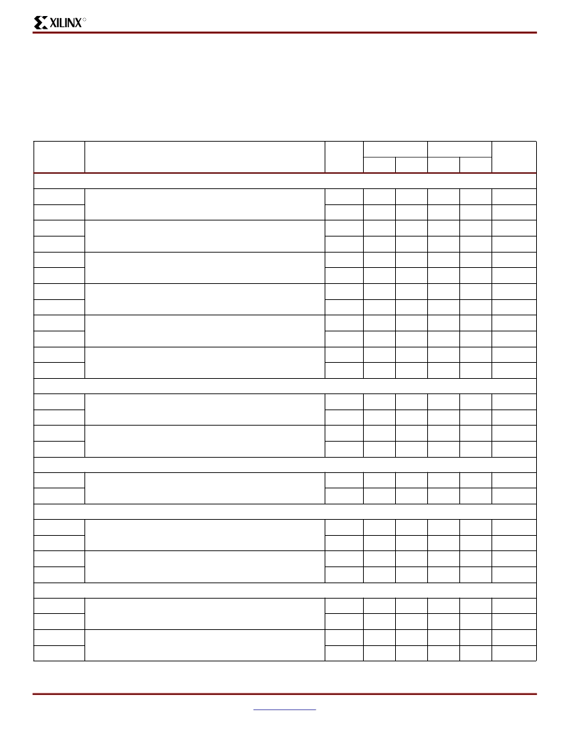
1-800-255-7778XQ4000E CLB Level-Sensitive RAM Switching Characteristic Guidelines
Testing of switching parameters is modeled after testing
methods specified by MIL-M-38510/605. All devices are
100% functionally tested. Internal timing parameters are
derived from measuring internal test patterns. Listed below
are representative values. For more specific, more precise,
and worst-case guaranteed data, use the values reported
by the static timing analyzer (TRCE in the Xilinx Develop-
ment System) and back-annotated to the simulation netlist.
All timing parameters assume worst-case operating condi-
tions (supply voltage and junction temperature). Values
apply to all XQ4000E devices unless otherwise noted.
Symbol
Single Port RAM
Size
-3
-4
Units
Min
Max
Min
Max
Write Operation
T
WC
T
WCT
T
WP
T
WPT
T
AS
T
AST
T
AH
T
AHT
T
DS
T
DST
T
DH
T
DHT
Read Operation
Address write cycle time
16x2
8.0
-
8.0
-
ns
32x1
8.0
-
8.0
-
ns
Write Enable pulse width (High)
16x2
4.0
-
4.0
-
ns
32x1
4.0
-
4.0
-
ns
Address setup time before WE
16x2
2.0
-
2.0
-
ns
32x1
2.0
-
2.0
-
ns
Address hold time after end of WE
16x2
2.0
-
2.5
-
ns
32x1
2.0
-
2.0
-
ns
D
IN
setup time before end of WE
16x2
2.2
-
4.0
-
ns
32x1
2.2
-
5.0
-
ns
D
IN
hold time after end of WE
16x2
2.0
-
2.0
-
ns
32x1
2.0
-
2.0
-
ns
T
RC
T
RCT
T
ILO
T
IHO
Address read cycle time
16x2
3.1
-
4.5
-
ns
32x1
5.5
-
6.5
-
ns
Data valid after address change (no Write Enable)
16x2
-
1.8
-
2.7
ns
32x1
-
3.2
-
4.7
ns
Read Operation, Clocking Data into Flip-Flop
T
ICK
T
IHCK
Read During Write
Address setup time before clock K
16x2
3.0
-
4.0
-
ns
32x1
4.6
-
6.1
-
ns
T
WO
T
WOT
T
DO
T
DOT
Read During Write, Clocking Data into Flip-Flop
Data valid after WE goes active (D
IN
stable before WE)
16x2
-
6.0
-
10.0
ns
32x1
-
7.3
-
12.0
ns
Data valid after D
IN
(D
IN
changes during WE)
16x2
-
6.6
-
9.0
ns
32x1
-
7.6
-
11.0
ns
T
WCK
T
WCKT
T
DCK
T
DOCK
Notes:
1.
Timing for the 16x1 RAM option is identical to 16x2 RAM timing.
WE setup time before clock K
16x2
6.0
-
8.0
-
ns
32x1
6.8
-
9.6
-
ns
Data setup time before clock K
16x2
5.2
-
7.0
-
ns
32x1
6.2
-
8.0
-
ns
相關(guān)PDF資料 |
PDF描述 |
|---|---|
| XQ4005E-4PG191N | QPRO XQ4000E/EX QML High-Reliability FPGAs |
| XQ4010E | QPRO XQ4000E/EX QML High-Reliability FPGAs |
| XQ4010E-3BG191M | QPRO XQ4000E/EX QML High-Reliability FPGAs |
| XQ4010E-3BG191N | QPRO XQ4000E/EX QML High-Reliability FPGAs |
| XQ4010E-3CB191M | QPRO XQ4000E/EX QML High-Reliability FPGAs |
相關(guān)代理商/技術(shù)參數(shù) |
參數(shù)描述 |
|---|---|
| XQ4005E-4PG191N | 制造商:XILINX 制造商全稱:XILINX 功能描述:QML High-Reliability FPGAs |
| XQ4005E-4PG196M | 制造商:XILINX 制造商全稱:XILINX 功能描述:QML High-Reliability FPGAs |
| XQ4005E-4PG196N | 制造商:XILINX 制造商全稱:XILINX 功能描述:QML High-Reliability FPGAs |
| XQ4005EX-3BG191M | 制造商:XILINX 制造商全稱:XILINX 功能描述:QML High-Reliability FPGAs |
| XQ4005EX-3BG191N | 制造商:XILINX 制造商全稱:XILINX 功能描述:QML High-Reliability FPGAs |
發(fā)布緊急采購,3分鐘左右您將得到回復(fù)。