- 您現(xiàn)在的位置:買賣IC網(wǎng) > PDF目錄376452 > XR-T56L22AD (EXAR CORP) Low Power Repeater/Receiver PDF資料下載
參數(shù)資料
| 型號: | XR-T56L22AD |
| 廠商: | EXAR CORP |
| 元件分類: | 數(shù)字傳輸電路 |
| 英文描述: | Low Power Repeater/Receiver |
| 中文描述: | DATACOM, PCM TRANSCEIVER, PDSO18 |
| 封裝: | 0.300 INCH, SOIC-18 |
| 文件頁數(shù): | 3/16頁 |
| 文件大小: | 344K |
| 代理商: | XR-T56L22AD |
XR-T56L22
3
Rev. 1.02
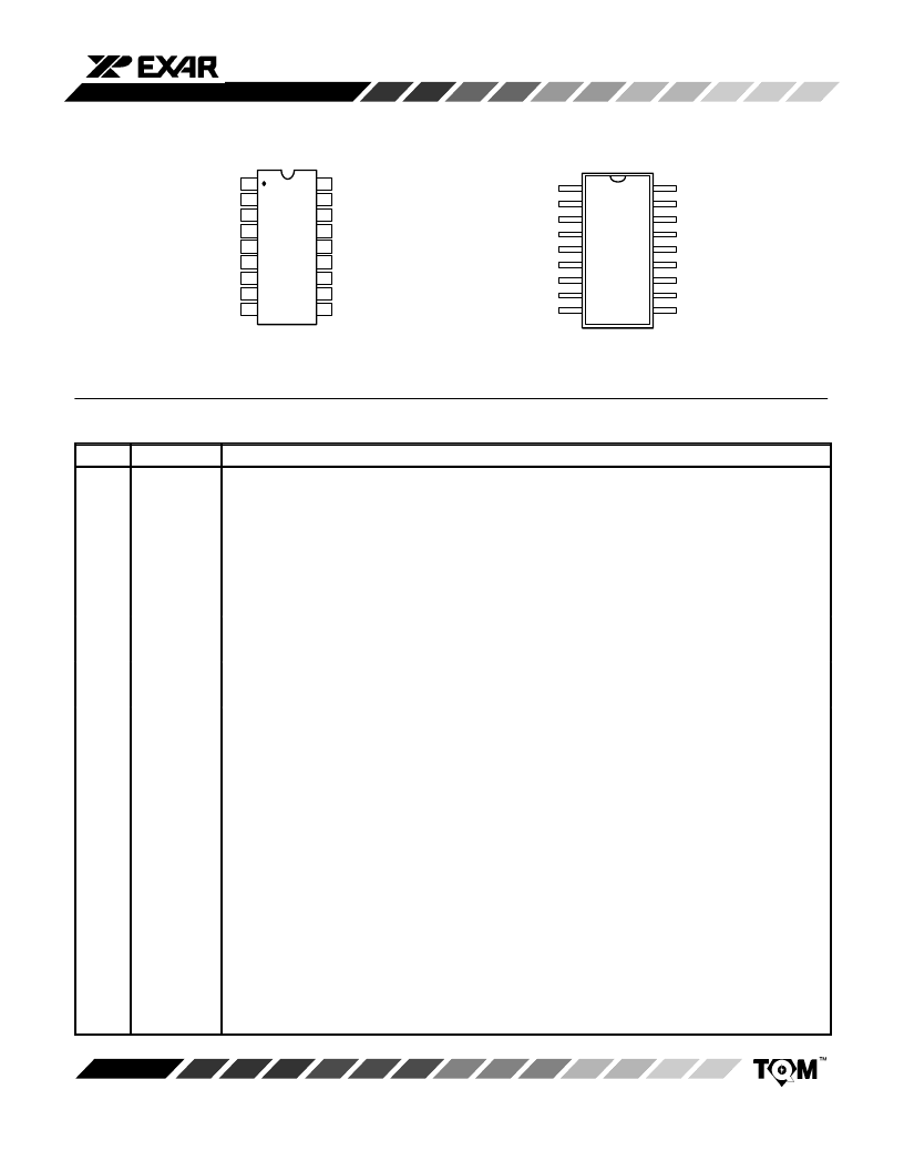
PIN CONFIGURATION
1
2
3
4
5
6
7
8
9
18
17
16
15
14
13
12
11
10
ALBO FIL
LC BIAS
LC I/P
PHASE CONT.
REG CONT.
V
REF
V
CC
CLOCK O/P
DATA-
ANA GND
ALBO1
ALBO2
AMP-I/P
AMP +I/P
AMP -O/P
AMP +O/P
DIG GND
DATA+
18 Lead PDIP, CDIP (0.300”)
18
1
10
9
2
3
4
5
6
7
15
14
13
12
11
17
16
8
ALBO FIL
LC BIAS
LC I/P
PHASE CONT.
REG CONT.
VREF
V
CC
CLOCK O/P
DATA-
ANA GND
ALBO1
ALBO2
AMP-I/P
AMP +I/P
AMP -O/P
AMP +O/P
DIG GND
DATA+
18 Lead SOIC (Jedec, 0.300”)
PIN DESCRIPTION
Pin #
Symbol
Description
1
ANA GND
Ground for Analog Sections of IC and Substrate.
2
ALBO 1
ALBO PORT 1 Output.
Port impedance varies between 25W and 20kW proportional to input signal
level.
ALBO PORT 2 Output.
Similar to pin 2.
3
ALBO 2
4
AMP - I/P
Inverting Input of Signal Preamp RIN > 20kW.
5
AMP + I/P
Non-Inverting Input of Signal Preamp. RIN > 20kW.
6
AMP - O/P
Inverting Output of Signal Pre-amp.
Rout < 200W. DC level typically 3.2V.
7
AMP + O/P
Non-inverting Output of Signal Pre-amp.
Similar to pin 6.
8
DIG GND
Ground for Digital Portion of IC.
9
DATA+
Positive Data Driver Output (Open Collector).
V
OL
< 0.95V @ l
OUT
= 32mA.
Negative Data Driver Output (Open Collector).
V
OL
< 0.95V @ l
OUT
= 32mA.
Phase Shifted Clock Output (Open Collector).
Decouple to GND with 0.1mF if not required. With
Rpull-up = 1K, V
OL
< 1.1V @ I
OUT
= 4mA.
Input Pin of Shunt Regulator and Supply Pin for IC.
For voltage feed applications the regulator
must be disabled and a 5V + 5% supply connected. For line feed a current of 48-120mA is required.
ICC < 8.75mA @ RON, ALBO = 25W typical.
10
DATA-
11
CLOCK O/P
12
V
CC
13
VREF
Output Voltage of Internal Reference of Shunt Regulator.
For parallel operation of regulators
should be tied to pin 13 of 2nd T56L22 device. V
REF
approxi-mately V
CC
/2. Decouple to GND with
0.1mF.
14
REG CONT
Input Voltage of Shunt Regulator Amp.
To inhibit regulator, pin should be tied to ground. For line
feed operation decouple to GND with 0.1mF. For parallel operation of regulators tie pin 14 of 2nd
T56L22 device. VREG approximately V
REF
.
Phase Shift Adjust Input.
A resistor to GND from the pin allows adjustment of phase shift from 905
to approximately 05. RP typical 1.8K to 1K. Vphase typical 340mV.
Clock Amplifier Input.
Pulsed with current from clock comparator. Connect LC tank between 16, 17
for clock recovery. Ickon = —110mA typical.
Clock Amplifier Reference Voltage.
VLC = 3.6V typical.
15
PHASE
CONT
LC I/P
16
17
LC BIAS
18
ALBO FIL
Control Pin for ALBO Ports.
Voltage developed across a capacitor on this pin defines ALBO on
impedance VALBO = 1.5V typical.
相關(guān)PDF資料 |
PDF描述 |
|---|---|
| XR-T56L22AN | Low Power Repeater/Receiver |
| XR-T56L22AP | Low Power Repeater/Receiver |
| XR-T56L85 | Low Power PCM Line Interface |
| XR-T56L85D | Low Power PCM Line Interface |
| XR-T56L85N | Low Power PCM Line Interface |
相關(guān)代理商/技術(shù)參數(shù) |
參數(shù)描述 |
|---|---|
| XR-T56L22AN | 制造商:EXAR 制造商全稱:EXAR 功能描述:Low Power Repeater/Receiver |
| XR-T56L22AP | 制造商:EXAR 制造商全稱:EXAR 功能描述:Low Power Repeater/Receiver |
| XR-T56L22ID | 制造商:未知廠家 制造商全稱:未知廠家 功能描述:PCM Repeater |
| XR-T56L22IN | 制造商:未知廠家 制造商全稱:未知廠家 功能描述:PCM Repeater |
| XR-T56L22IP | 制造商:未知廠家 制造商全稱:未知廠家 功能描述:PCM Repeater |
發(fā)布緊急采購,3分鐘左右您將得到回復(fù)。