- 您現(xiàn)在的位置:買賣IC網(wǎng) > PDF目錄16513 > XR19L200IL32-0B-EB (Exar Corporation)EVAL BOARD FOR XR19L200 32QFN PDF資料下載
參數(shù)資料
| 型號(hào): | XR19L200IL32-0B-EB |
| 廠商: | Exar Corporation |
| 文件頁數(shù): | 39/40頁 |
| 文件大小: | 0K |
| 描述: | EVAL BOARD FOR XR19L200 32QFN |
| 標(biāo)準(zhǔn)包裝: | 1 |
| 系列: | * |
第1頁第2頁第3頁第4頁第5頁第6頁第7頁第8頁第9頁第10頁第11頁第12頁第13頁第14頁第15頁第16頁第17頁第18頁第19頁第20頁第21頁第22頁第23頁第24頁第25頁第26頁第27頁第28頁第29頁第30頁第31頁第32頁第33頁第34頁第35頁第36頁第37頁第38頁當(dāng)前第39頁第40頁

XR19L200
8
SINGLE CHANNEL INTEGRATED UART AND RS-232 TRANSCEIVER
REV. 1.0.2
2.8
Crystal or External Clock Input
The L200 includes an on-chip oscillator (XTAL1 and XTAL2) to generate a clock when a crystal is connected
between the XTAL1 and XTAL2 pins of the device. Alternatively, an external clock can be supplied through the
XTAL1 pin. The CPU data bus does not require this clock for bus operation. The crystal oscillator provides a
system clock to the Baud Rate Generators (BRG) section found in each of the UART. XTAL1 is the input to the
oscillator or external clock input and XTAL2 pin is the bufferred output which can be used as a clock signal for
other devices in the system. Please note that the input XTAL1 is not 5V tolerant and therefore, the maximum
voltage at the pin should be VCC when an external clock is supplied. For programming details, see
“Programmable Baud Rate Generator.”
The on-chip oscillator is designed to use an industry standard microprocessor crystal (parallel resonant,
fundamental frequency with 10-22 pF capacitance load, ESR of 20-120 ohms and 100ppm frequency
tolerance) connected externally between the XTAL1 and XTAL2 pins. When VCC = 5V, the on-chip oscillator
can operate with a crystal whose frequency is not greater than 24 MHz. On the other hand, the L200 can
accept an external clock of up to 50MHz at XTAL1 pin also. Although the L200 can accept an exteran clock of
up to 50MHz, the maximum data rate supported by the RS-232 drivers is 250Kbps. For further reading on the
oscillator circuit please see the Application Note DAN108 on the EXAR web site at http://www.exar.com.
2.9
Programmable Baud Rate Generator
The L200 UART has its own Baud Rate Generator (BRG) with a prescaler. The prescaler is controlled by a
software bit (bit-7) in the MCR register. This bit selects the prescaler to divide the input crystal or external clock
by a factor of 1 or 4. The clock output of the prescaler goes to the BRG. The BRG further divides this clock by
a programmable divisor (via DLL and DLM registers) between 1 and (216 -1) to obtain a 16X sampling rate
clock of the serial data rate. The sampling rate clock is used by the transmitter for data bit shifting and receiver
for data sampling. The BRG divisor defaults to the maximum baud rate (DLL = 0x01 and DLM = 0x00) upon
power up.
TABLE 2: INT (IRQ#) PIN OPERATION FOR RECEIVER
FCR BIT-0 = 0
(FIFO DISABLED)
FCR BIT-0 = 1
(FIFO ENABLED)
INT Pin
(I/M# = 1)
0 = no data
1 = 1 byte
0 = FIFO below trigger level
1 = FIFO above trigger level
IRQ# Pin
(I/M# = 0)
1 = no data
0 = 1 byte
1 = FIFO below trigger level
0 = FIFO above trigger level
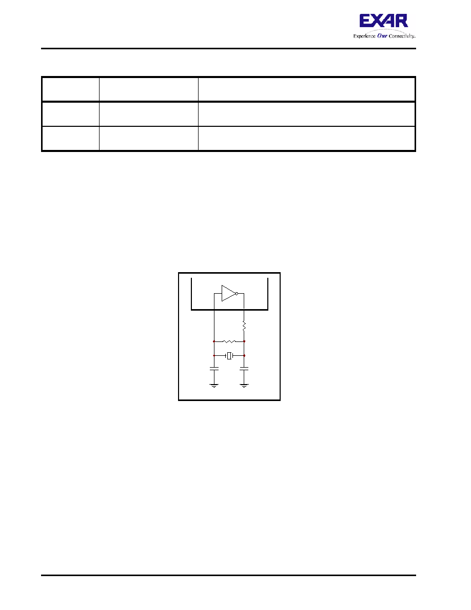
FIGURE 4. TYPICAL CRYSTAL CONNECTIONS
C1
22-47pF
C2
22-47pF
Y1
1.8432 MHz
to
24 MHz
R1
0-120
(Optional)
R2
500K - 1M
XTAL1
XTAL2
相關(guān)PDF資料 |
PDF描述 |
|---|---|
| VI-JVK-EZ-S | CONVERTER MOD DC/DC 40V 25W |
| 6374615-9 | C/A LC-SC DUP 62.5/125, 9M |
| ESC12DRTH-S13 | CONN EDGECARD 24POS .100 EXTEND |
| VE-JTK-EX | CONVERTER MOD DC/DC 40V 75W |
| 1-5503995-0 | CA 62.5/125UM ZIP OMCER 1.22 |
相關(guān)代理商/技術(shù)參數(shù) |
參數(shù)描述 |
|---|---|
| XR19L200IL32-F | 功能描述:UART 接口集成電路 UART RoHS:否 制造商:Texas Instruments 通道數(shù)量:2 數(shù)據(jù)速率:3 Mbps 電源電壓-最大:3.6 V 電源電壓-最小:2.7 V 電源電流:20 mA 最大工作溫度:+ 85 C 最小工作溫度:- 40 C 封裝 / 箱體:LQFP-48 封裝:Reel |
| XR19L202 | 制造商:EXAR 制造商全稱:EXAR 功能描述:TWO CHANNEL INTEGRATED UART AND RS-232 TRANSCEIVER |
| XR19L202IL48 | 制造商:EXAR 制造商全稱:EXAR 功能描述:TWO CHANNEL INTEGRATED UART AND RS-232 TRANSCEIVER |
| XR19L202IL48-0B-EB | 功能描述:界面開發(fā)工具 Supports L202 48 pin QFN,PCI Interface RoHS:否 制造商:Bourns 產(chǎn)品:Evaluation Boards 類型:RS-485 工具用于評(píng)估:ADM3485E 接口類型:RS-485 工作電源電壓:3.3 V |
| XR19L202IL48-F | 功能描述:UART 接口集成電路 UART RoHS:否 制造商:Texas Instruments 通道數(shù)量:2 數(shù)據(jù)速率:3 Mbps 電源電壓-最大:3.6 V 電源電壓-最小:2.7 V 電源電流:20 mA 最大工作溫度:+ 85 C 最小工作溫度:- 40 C 封裝 / 箱體:LQFP-48 封裝:Reel |
發(fā)布緊急采購,3分鐘左右您將得到回復(fù)。