- 您現(xiàn)在的位置:買賣IC網(wǎng) > PDF目錄48107 > YNV05T10025-0G (POWER-ONE INC) 1-OUTPUT DC-DC REG PWR SUPPLY MODULE PDF資料下載
參數(shù)資料
| 型號(hào): | YNV05T10025-0G |
| 廠商: | POWER-ONE INC |
| 元件分類: | 電源模塊 |
| 英文描述: | 1-OUTPUT DC-DC REG PWR SUPPLY MODULE |
| 文件頁數(shù): | 26/26頁 |
| 文件大小: | 435K |
| 代理商: | YNV05T10025-0G |
第1頁第2頁第3頁第4頁第5頁第6頁第7頁第8頁第9頁第10頁第11頁第12頁第13頁第14頁第15頁第16頁第17頁第18頁第19頁第20頁第21頁第22頁第23頁第24頁第25頁當(dāng)前第26頁
OCT 17, 2006 revised to APR 11, 2007
Page 9 of 26
www.power-one.com
YNV05T100xy DC-DC Converter Family Data Sheet
3.0-5.5 VDC Input; 0.9-3.3 VDC Output @ 10A
varied between 25 °C and 85 °C, with airflow rates
from 30 to 500 LFM (0.15 m/s to 2.5 m/s), and
vertical and horizontal converter mounting. The
airflow during the testing is parallel to the long axis
of the converter, going from ON/OFF pin to output
pins.
For each set of conditions, the maximum load
current was defined as the lowest of:
(i) The output current at which any MOSFET
temperature does not exceed a maximum
specified temperature (120 °C) as indicated by the
thermographic image, or
(ii) The maximum current rating of the converter
(10 A)
During normal operation, derating curves with
maximum FET temperature less than or equal to
120 °C should not be exceeded. Temperature on
the PCB at the thermocouple locations shown in
Fig. G should not exceed 120 °C in order to
operate inside the derating curves.
Efficiency
Fig. x.3 show the efficiency vs. load current plot for
ambient temperature of 25 C, airflow rate of 200
LFM (1 m/s) and input voltages of 4.5 V, 5.0 V,
and 5.5 V.
Fig. x.4 show the efficiency vs. load current plot for
ambient temperature of 25 C, airflow rate of 200
LFM (1 m/s) and input voltages of 3.0 V, 3.3 V,
and 3.6 V for output voltages
≤ 2.5 V.
Power Dissipation
Fig. 3.3V.4 shows the power dissipation vs. load
current plot for Ta = 25 C, airflow rate of 200 LFM
(1 m/s) with vertical mounting and input voltages
of 4.5 V, 5.0 V, and 5.5 V for 3.3 V output voltage.
Start-up
Output voltage waveforms, during the turn-on
transient with application of Vin at full rated load
current (resistive load) are shown with 47
μF
external load capacitance at Vin = 5 V in Fig. x.5.
Ripple and Noise
The output voltage ripple waveform is measured at
full rated load current. Note that all output voltage
waveforms are measured across a 1
μF ceramic
capacitor.
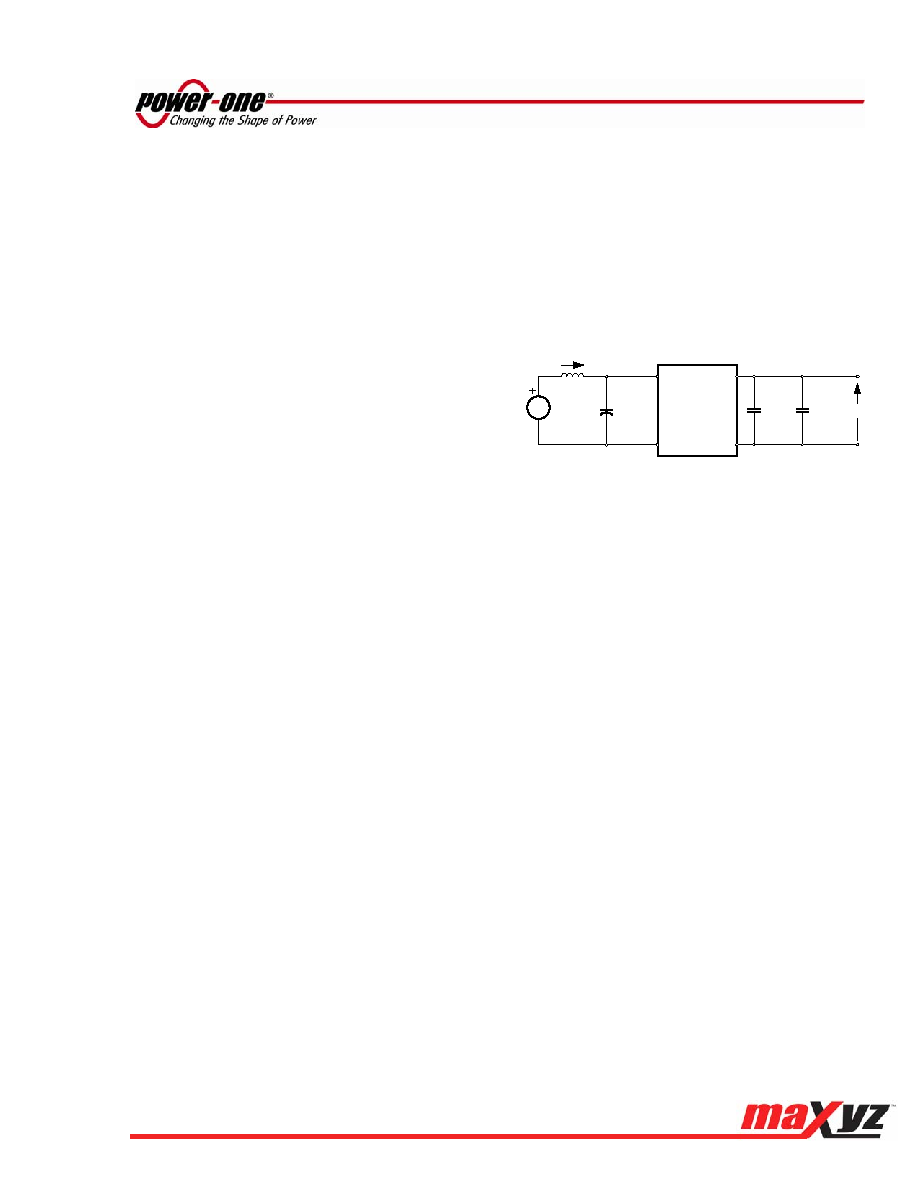
The output voltage ripple and input reflected ripple
current waveforms are obtained using the test
setup shown in Fig. H.
i
S
Vout
Vsource
1
μF
ceramic
capacitor
1
μH
source
inductance
DC/DC
Converter
4 x 47
μF
ceramic
capacitor
47
μF
ceramic
capacitor
C
O
C
IN
Nex -v Series
TM
Vin
GND
Vout
Fig. H: Test setup for measuring input reflected ripple
currents,
is and output voltage ripple.
相關(guān)PDF資料 |
PDF描述 |
|---|---|
| YNV05T10020-0 | 1-OUTPUT DC-DC REG PWR SUPPLY MODULE |
| YNV05T10025-D | 1-OUTPUT DC-DC REG PWR SUPPLY MODULE |
| YNV05T10009-D | 1-OUTPUT DC-DC REG PWR SUPPLY MODULE |
| YNV05T10020-0G | 1-OUTPUT DC-DC REG PWR SUPPLY MODULE |
| YNV05T10009-DG | 1-OUTPUT DC-DC REG PWR SUPPLY MODULE |
相關(guān)代理商/技術(shù)參數(shù) |
參數(shù)描述 |
|---|---|
| YNV05T10025-DG | 制造商:Power-One 功能描述:DC/DC PS SGL-OUT 25V 10A 36.3W 10SIP - Bulk |
| YNV05T10033-0G | 制造商:Power-One 功能描述:DC/DC PS SGL-OUT 3.3V 10A 36.3W 10SIP - Bulk |
| YNV05T10033-D | 功能描述:DC/DC轉(zhuǎn)換器 RoHS:否 制造商:Murata 產(chǎn)品: 輸出功率: 輸入電壓范圍:3.6 V to 5.5 V 輸入電壓(標(biāo)稱): 輸出端數(shù)量:1 輸出電壓(通道 1):3.3 V 輸出電流(通道 1):600 mA 輸出電壓(通道 2): 輸出電流(通道 2): 安裝風(fēng)格:SMD/SMT 封裝 / 箱體尺寸: |
| YNV05T10033-D02G | 制造商:Power-One 功能描述: |
| YNV05T10033-D03G | 制造商:Power-One 功能描述: |
發(fā)布緊急采購,3分鐘左右您將得到回復(fù)。