- 您現(xiàn)在的位置:買賣IC網(wǎng) > PDF目錄373766 > Z86C0208PEC (ZILOG INC) LOW-COST, 512-BYTE ROM MICROCONTROLLERS PDF資料下載
參數(shù)資料
| 型號: | Z86C0208PEC |
| 廠商: | ZILOG INC |
| 元件分類: | 微控制器/微處理器 |
| 英文描述: | LOW-COST, 512-BYTE ROM MICROCONTROLLERS |
| 中文描述: | 8-BIT, MROM, 8 MHz, MICROCONTROLLER, PDIP18 |
| 封裝: | PLASTIC, DIP-18 |
| 文件頁數(shù): | 5/36頁 |
| 文件大?。?/td> | 898K |
| 代理商: | Z86C0208PEC |
第1頁第2頁第3頁第4頁當(dāng)前第5頁第6頁第7頁第8頁第9頁第10頁第11頁第12頁第13頁第14頁第15頁第16頁第17頁第18頁第19頁第20頁第21頁第22頁第23頁第24頁第25頁第26頁第27頁第28頁第29頁第30頁第31頁第32頁第33頁第34頁第35頁第36頁
Z86C02/E02/L02
Low-Cost, 512-Byte ROM Microcontrollers
DS96DZ80301 (11/96)
P R E L I M I N A R Y
1-5
1
ABSOLUTE MAXIMUM RATINGS
Notes:
Stresses greater than those listed under Absolute
Maximum Ratings may cause permanent damage to the
device. This is a stress rating only; functional operation of
the device at any condition above those indicated in the
operational sections of these specifications is not implied.
Exposure to absolute maximum rating conditions for an
extended period may affect device reliability.
Total power dissipation should not exceed 462 mW for the
package. Power dissipation is calculated as follows:
1.
This applies to all pins except where otherwise noted.
2.
Maximum current into pin must be
There is no input protection diode from pin to V
±
600
μ
A.
DD
.
3.
This excludes Pin 6 and Pin 7.
4.
Device pin is not at an output Low state.
Total Power dissipation = V
DD
x [I
DD
– (sum of I
OH
)] + sum of [(V
DD
– V
OH
) x I
OH
] + sum of (V
0L
x I
0L
)
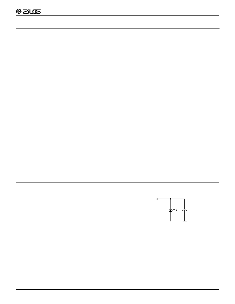
STANDARD TEST CONDITIONS
The characteristics listed below apply for standard test
conditions as noted. All voltages are referenced to
Ground. Positive current flows into the referenced pin (Fig-
ure 6).
CAPACITANCE
T
A
= 25
°
C, V
CC
= GND = 0V, f = 1.0 MHz, unmeasured pins returned to GND.
Parameter
Ambient Temperature under Bias
Storage Temperature
Voltage on any Pin with Respect to V
Voltage on V
DD
Pin with Respect to V
Voltage on Pin 7 with Respect to V
Voltage on Pin 7,8,9,10 with Respect to V
Total Power Dissipation
Maximum Allowed Current out of V
Maximum Allowed Current into V
Maximum Allowed Current into an Input Pin [Note 3]
Maximum Allowed Current into an Open-Drain Pin [Note 4]
Maximum Allowed Output Current Sinked by Any I/O Pin
Maximum Allowed Output Current Sourced by Any I/O Pin
Maximum Allowed Output Current Sinked by Port 2, Port 0
Maximum Allowed Output Current Sourced by Port 2, Port 0
Min
–40
–65
–0.7
–0.3
–0.7
–0.7
Max
+105
+150
+12
+7
V
DD
V
DD
462
300
270
+600
+600
20
20
80
80
Units
C
C
V
V
V
V
mW
mA
mA
μ
A
μ
A
mA
mA
mA
mA
SS
[Note 1]
SS
[Note 2] (Z86C02/L02)
[Note 2] (Z86E02)
SS
+1
+1
SS
SS
DD
–600
–600
Figure 6. Test Load Diagram
From Output
Under Test
150 pF
Parameter
Input capacitance
Output capacitance
I/O capacitance
Min
0
0
0
Max
15 pF
20 pF
25 pF
相關(guān)PDF資料 |
PDF描述 |
|---|---|
| Z86L02 | LOW-COST, 512-BYTE ROM MICROCONTROLLERS |
| Z86L0208PEC | LOW-COST, 512-BYTE ROM MICROCONTROLLERS |
| Z86L0208PSC | LOW-COST, 512-BYTE ROM MICROCONTROLLERS |
| Z86L0208SEC | LOW-COST, 512-BYTE ROM MICROCONTROLLERS |
| Z86L0208SSC | LOW-COST, 512-BYTE ROM MICROCONTROLLERS |
相關(guān)代理商/技術(shù)參數(shù) |
參數(shù)描述 |
|---|---|
| Z86C0208PSC | 制造商:ZILOG 制造商全稱:ZILOG 功能描述:LOW-COST, 512-BYTE ROM MICROCONTROLLERS |
| Z86C0208SEC | 制造商:ZILOG 制造商全稱:ZILOG 功能描述:LOW-COST, 512-BYTE ROM MICROCONTROLLERS |
| Z86C0208SSC | 制造商:ZILOG 制造商全稱:ZILOG 功能描述:LOW-COST, 512-BYTE ROM MICROCONTROLLERS |
| Z86C0208SSCR3808 | 制造商:Zilog Inc 功能描述: |
| Z86C0208SSCR3808TR | 制造商:Zilog Inc 功能描述: |
發(fā)布緊急采購,3分鐘左右您將得到回復(fù)。