- 您現(xiàn)在的位置:買(mǎi)賣(mài)IC網(wǎng) > PDF目錄373766 > Z86C0208SEC (ZILOG INC) LOW-COST, 512-BYTE ROM MICROCONTROLLERS PDF資料下載
參數(shù)資料
| 型號(hào): | Z86C0208SEC |
| 廠(chǎng)商: | ZILOG INC |
| 元件分類(lèi): | 微控制器/微處理器 |
| 英文描述: | LOW-COST, 512-BYTE ROM MICROCONTROLLERS |
| 中文描述: | 8-BIT, MROM, 8 MHz, MICROCONTROLLER, PDSO18 |
| 封裝: | SOIC-18 |
| 文件頁(yè)數(shù): | 19/36頁(yè) |
| 文件大小: | 898K |
| 代理商: | Z86C0208SEC |
第1頁(yè)第2頁(yè)第3頁(yè)第4頁(yè)第5頁(yè)第6頁(yè)第7頁(yè)第8頁(yè)第9頁(yè)第10頁(yè)第11頁(yè)第12頁(yè)第13頁(yè)第14頁(yè)第15頁(yè)第16頁(yè)第17頁(yè)第18頁(yè)當(dāng)前第19頁(yè)第20頁(yè)第21頁(yè)第22頁(yè)第23頁(yè)第24頁(yè)第25頁(yè)第26頁(yè)第27頁(yè)第28頁(yè)第29頁(yè)第30頁(yè)第31頁(yè)第32頁(yè)第33頁(yè)第34頁(yè)第35頁(yè)第36頁(yè)
Z86C02/E02/L02
Low-Cost, 512-Byte ROM Microcontrollers
DS96DZ80301 (11/96)
P R E L I M I N A R Y
1-19
1
FUNCTIONAL DESCRIPTION
The following special functions have been incorporated
into the Z86C02/E02/L02 devices to enhance the standard
Z8
core architecture to provide the user with increased de-
sign flexibility.
RESET.
This function is accomplished by means of a Pow-
er-On Reset or a Watch-Dog Timer Reset. Upon power-
up, the Power-On Reset circuit waits for T
POR
ms, plus 18
clock cycles, then starts program execution at address
000C (Hex) (Figure 11). The control registers' reset value
is shown in Table 4.
Power-On Reset (POR).
A timer circuit clocked by a ded-
icated on-board RC oscillator is used for a POR timer func-
tion. The POR time allows V
CC
and the oscillator circuit to
stabilize before instruction execution begins. The POR
timer circuit is a one-shot timer triggered by one of the four
following conditions:
I
Power bad to power good status
I
Stop-Mode Recovery
I
WDT time-out
I
WDH time-out (in Halt Mode)
I
WDT time-out (in Stop Mode)
Watch-Dog Timer Reset.
The WDT is a retriggerable
one-shot timer that resets the Z8 if it reaches its terminal
count. The WDT is initially enabled by executing the WDT
instruction and is retriggered on subsequent execution of
the WDT instruction. The timer circuit is driven by an on-
board RC oscillator. If the permanent WDT option is select-
ed then the WDT is enabled after reset and operates in
RUN Mode, HALT mode, STOP mode and cannot be dis-
abled. If the permanent WDT option is not selected then
the WDT, when enabled by the user's software, does not
operate in STOP Mode, but it can operate in HALT Mode
by using a WDH instruction.
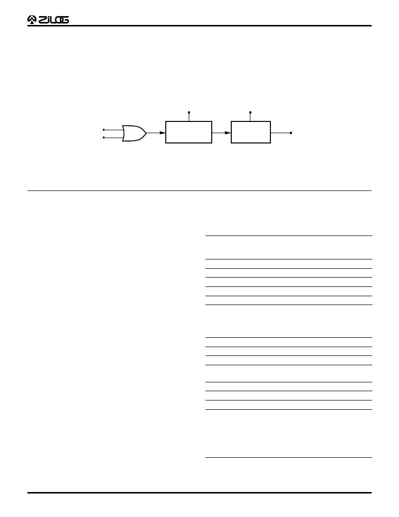
Figure 11. Internal Reset Configuration
POR
(Cold Start)
P27
(Stop Mode)
Delay Line
T
POR
ms
18 CLK
Reset Filter
Chip
Reset
XTAL OSC
INT OSC
Table 4. Control Register
Reset Condition
Addr Reg.
FF
FE
FD
FC
FB
FA
D7 D6 D5 D4 D3 D2 D1 D0 Comments
0
0
0
0
0
0
0
0
0
0
0
0
0
0
0
0
0
0
FLAGS U
U
U
U
U
IMR
0
U
U
U
U
IRQ
U
U
0
0
0
SPL
GPR
RP
0
0
0
U
U
0
0
0
0
U
U
0 IRQ3 is used
for positive
edge
detection
U
1
0 P2 open-drain
1 Inputs after
reset
0
U
0
U
U
0
F9
F8
F7*
F6*
IPR
P01M
P3M
P2M
U
U
U
1
U
U
U
1
U
U
U
1
U
0
U
1
U
U
U
1
U
U
U
1
U
0
0
1
F3
F2
F1
Note:
*Registers are not reset after a STOP-Mode Recovery
using P27 pin. A subsequent reset will cause these control
registers to be reconfigured as shown in Table 4 and the
user must avoid bus contention on the port pins or it may
affect device reliability.
PRE1
T1
TMR
U
U
0
U
U
0
U
U
0
U
U
0
U
U
0
U
U
0
0
U
0
相關(guān)PDF資料 |
PDF描述 |
|---|---|
| Z86C0208SSC | LOW-COST, 512-BYTE ROM MICROCONTROLLERS |
| Z86C02 | Cost Effective ,512-Byte ROM CMOS Z8 Microcontroller(帶512字節(jié)ROM的CMOS 微控制器) |
| Z86C06 | CMOS Z8 8-BIT CCP CONSUMER CONTROLLER PROCESSORS |
| Z86C03 | CMOS Z8 8-BIT CCP CONSUMER CONTROLLER PROCESSORS |
| Z86C08 | CMOS 8-BIT LOW-COST 1K/2K-ROM MICROCONTROLLERS |
相關(guān)代理商/技術(shù)參數(shù) |
參數(shù)描述 |
|---|---|
| Z86C0208SSC | 制造商:ZILOG 制造商全稱(chēng):ZILOG 功能描述:LOW-COST, 512-BYTE ROM MICROCONTROLLERS |
| Z86C0208SSCR3808 | 制造商:Zilog Inc 功能描述: |
| Z86C0208SSCR3808TR | 制造商:Zilog Inc 功能描述: |
| Z86C0208SSGR3808TR | 制造商:Zilog Inc 功能描述: |
| Z86C03 | 制造商:ZILOG 制造商全稱(chēng):ZILOG 功能描述:CMOS Z8 8-BIT CCP CONSUMER CONTROLLER PROCESSORS |
發(fā)布緊急采購(gòu),3分鐘左右您將得到回復(fù)。