- 您現(xiàn)在的位置:買賣IC網(wǎng) > PDF目錄373767 > Z86C8416SEC (ZILOG INC) Z8 MCU MICROCONTROLLERS PDF資料下載
參數(shù)資料
| 型號: | Z86C8416SEC |
| 廠商: | ZILOG INC |
| 元件分類: | 微控制器/微處理器 |
| 英文描述: | Z8 MCU MICROCONTROLLERS |
| 中文描述: | 8-BIT, MROM, 16 MHz, MICROCONTROLLER, PDSO28 |
| 封裝: | PLASTIC, SOIC-28 |
| 文件頁數(shù): | 30/46頁 |
| 文件大小: | 957K |
| 代理商: | Z86C8416SEC |
第1頁第2頁第3頁第4頁第5頁第6頁第7頁第8頁第9頁第10頁第11頁第12頁第13頁第14頁第15頁第16頁第17頁第18頁第19頁第20頁第21頁第22頁第23頁第24頁第25頁第26頁第27頁第28頁第29頁當前第30頁第31頁第32頁第33頁第34頁第35頁第36頁第37頁第38頁第39頁第40頁第41頁第42頁第43頁第44頁第45頁第46頁
Z86C83/C84
Z8
MCU Microcontrollers
30
DS96DZ80203
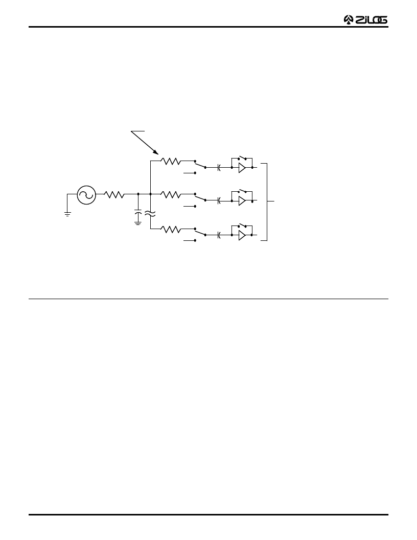
Figure 27 shows the input circuit of the ADC. When
conversion starts the analog input voltage is connected to
the MSB and LSB flash converter inputs as shown in the
Input Impedance CKT diagram. Effectively, shunting 31
parallel internal resistance of the analog switches and
simultaneously charging 31 parallel 0.5 pF capacitors,
which is equivalent to seeing a 400 Ohms input impedance
in parallel with a 16 pF capacitor. Other input stray
capacitance adds about 10 pF to the input load. For input
source resistances up to 2 kOhms can be used under
normal operating condition without any degradation of the
input settling time. For larger input source resistance,
longer conversion cycle time may be required to
compensate the input settling time problem.
Typical Z8 A/D Conversion Sequence
1.
Set the register pointer to Extended Bank (C),that is,
SRP #%0C instruction.
2.
Next, set ADE flag by loading ADC1 Control Register
Bank (C) Register 9, bit 7. Also, load bits 0-4 of this
same register to select a AV
or A
offset value. A
precision voltage divider connected to the A/D
resistive ladder can offset conversion dynamic range
to specified limits within the AV
and A
limits. By
loading Bank (C) Register 9, bits 0-4, with the
appropriate value it is possible to select from these
groups:
a.
No Offset. The Converter Dynamic range is from
0V to 5.0V for AV
CC
= 5.0V.
b.
35 Percent A
Offset. The Converter Dynamic
range is 1.75V - 5.0V for AV
CC
= 5.0V.
c.
50 Percent A
Offset. The Converter Dynamic
range is 2.5V - 5.0V for AV
CC
= 5.0V.
3.
Select one of the eight A/D inputs for conversion by
loading Bank (C) Register 8 with the desired attributes:
Bits 0 - 2 select an A/D input, bits 3 and 4 select A/D
conversion (or digital port I/O).
4.
Set Bank (C) Register 8, bit 3 to enable A/D
conversion. (This flag can be set concurrently with
step 3.) This flag is automatically reset when the A/D
conversion is completed, so a bit test can be
performed to determine A/D readiness if necessary.
5.
Read the A/D result in Bank (C) Register A. Please
note that the A/D result is not valid (indeterminate)
unless ADE flag (Register 9, bit 7) was previously set,
otherwise A/D converter output is tri-stated.
Figure 27. Input Impedance of ADC
CMOS Switch
on Resistance
2 - 5 k
C Parasitic
R Source
C .5 pF
V Ref
C .5 pF
C .5 pF
31 CMOS Digital
Comparators
V Ref
V Ref
相關PDF資料 |
PDF描述 |
|---|---|
| Z86C8416SSC | Z8 MCU MICROCONTROLLERS |
| Z86C8416VEC | Z8 MCU MICROCONTROLLERS |
| Z86C8416VSC | Z8 MCU MICROCONTROLLERS |
| Z86C84 | Z8 MCU MICROCONTROLLERS |
| Z86C83 | CMOS Z8 Microcontroller(CMOS Z8系列微控制器) |
相關代理商/技術參數(shù) |
參數(shù)描述 |
|---|---|
| Z86C8416SSC | 制造商:ZILOG 制造商全稱:ZILOG 功能描述:Z8 MCU MICROCONTROLLERS |
| Z86C8416VEC | 制造商:ZILOG 制造商全稱:ZILOG 功能描述:Z8 MCU MICROCONTROLLERS |
| Z86C8416VSC | 制造商:ZILOG 制造商全稱:ZILOG 功能描述:Z8 MCU MICROCONTROLLERS |
| Z86C89 | 制造商:ZILOG 制造商全稱:ZILOG 功能描述:ROMLESS CMOS Z8 8-BIT MICROCONTROLLER |
| Z86C89-08FEC | 制造商:未知廠家 制造商全稱:未知廠家 功能描述:8-Bit Microcontroller |
發(fā)布緊急采購,3分鐘左右您將得到回復。