- 您現(xiàn)在的位置:買賣IC網(wǎng) > PDF目錄372962 > Z86E0812SSC1924 (ZILOG INC) CMOS Z8 OTP Microcontrollers PDF資料下載
參數(shù)資料
| 型號: | Z86E0812SSC1924 |
| 廠商: | ZILOG INC |
| 元件分類: | 微控制器/微處理器 |
| 英文描述: | CMOS Z8 OTP Microcontrollers |
| 中文描述: | 8-BIT, OTPROM, 12 MHz, MICROCONTROLLER, PDSO18 |
| 封裝: | PLASTIC, SOIC-18 |
| 文件頁數(shù): | 26/44頁 |
| 文件大小: | 251K |
| 代理商: | Z86E0812SSC1924 |
第1頁第2頁第3頁第4頁第5頁第6頁第7頁第8頁第9頁第10頁第11頁第12頁第13頁第14頁第15頁第16頁第17頁第18頁第19頁第20頁第21頁第22頁第23頁第24頁第25頁當(dāng)前第26頁第27頁第28頁第29頁第30頁第31頁第32頁第33頁第34頁第35頁第36頁第37頁第38頁第39頁第40頁第41頁第42頁第43頁第44頁
Z86E04/E08
CMOS Z8 OTP Microcontrollers
Zilog
26
P R E L I M I N A R Y
DS97Z8X0401
FUNCTIONAL DESCRIPTION
(Continued)
The Z86E04/E08 instructions can access registers directly
or indirectly through an 8-bit address field. This allows
short 4-bit register addressing using the Register Pointer.
In the 4-bit mode, the register file is divided into eight work-
ing register groups, each occupying 16 continuous loca-
tions. The Register Pointer (Figure 13) addresses the
starting location of the active working-register group.
Stack Pointer.
The Z86E04/E08 has an 8-bit Stack Point-
er (R255) used for the internal stack that resides within the
124 general-purpose registers.
General-Purpose Registers (GPR).
These registers are
undefined after the device is powered up. The registers
keep their last value after any reset, as long as the reset
occurs in the V
CC
voltage-specified operating range.
Note:
Register R254 has been designated as a general-purpose
register and is set to 00 Hex after any reset or Stop-Mode
Recovery.
Counter/Timer.
There are two 8-bit programmable
counter/timers (T0 and T1), each driven by its own 6-bit
programmable prescaler. The T1 prescaler is driven by in-
ternal or external clock sources; however, the T0 can be
driven by the internal clock source only (Figure 15).
The 6-bit prescalers divide the input frequency of the clock
source by any integer number from 1 to 64. Each prescaler
drives its counter, which decrements the value (1 to 256)
that has been loaded into the counter. When both counter
and prescaler reach the end of count, a timer interrupt re-
quest IRQ4 (T0) or IRQ5 (T1) is generated.
The counter can be programmed to start, stop, restart to
continue, or restart from the initial value. The counters are
also programmed to stop upon reaching zero (Single-Pass
Mode) or to automatically reload the initial value and con-
tinue counting (Modulo-N Continuous Mode).
The counters, but not the prescalers, are read at any time
without disturbing their value or count mode. The clock
source for T1 is user-definable and is either the internal mi-
croprocessor clock divided by four, or an external signal in-
put through Port 3. The Timer Mode register configures the
external timer input (P31) as an external clock, a trigger in-
put that is retriggerable or non-retriggerable, or used as a
gate input for the internal clock.
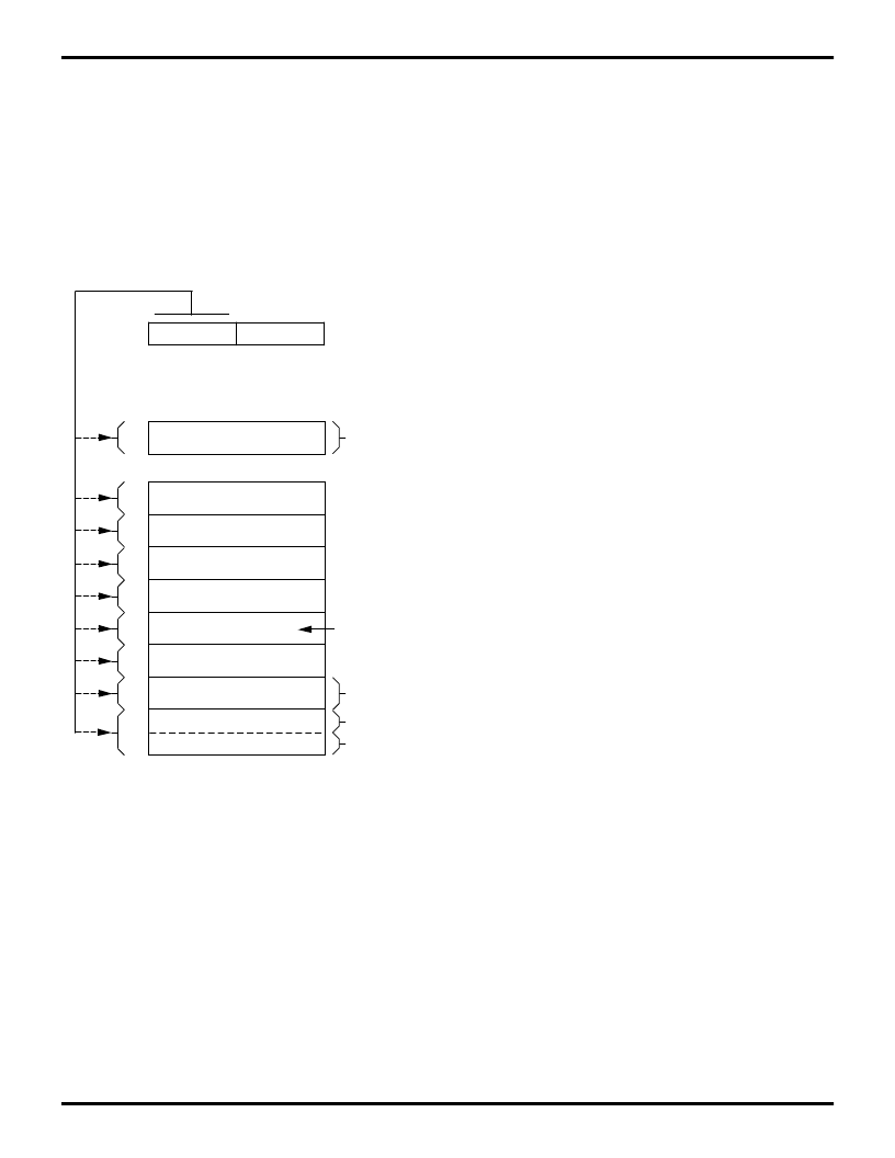
Figure 13. Register Pointer
The upper nibble of the register file address
provided by the register pointer specifies
the active working-register group.
r7
r6
r5
r4
R253
(Register Pointer)
I/O Ports
Specified Working
Register Group
The lower nibble
of the register
file address
provided by the
instruction points
to the specified
register.
r3
r2
r1
r0
Register Group 1
Register Group 0
R15 to R0
Register Group F
R15 to R4*
R3 to R0
R15 to R0
FF
F0
0F
00
1F
10
2F
20
3F
30
4F
40
5F
50
6F
60
7F
70
*Expanded Register Group (0) is selected in this figure
by handling bits D3 to D0 as "0" in Register R253(RP).
相關(guān)PDF資料 |
PDF描述 |
|---|---|
| Z86E0412PSC1860 | CMOS Z8 OTP Microcontrollers |
| Z86E0412PSC1866 | CMOS Z8 OTP Microcontrollers |
| Z86E0412PSC1903 | CMOS Z8 OTP Microcontrollers |
| Z86E0412PSC1924 | CMOS Z8 OTP Microcontrollers |
| Z86E0412SEC | CMOS Z8 OTP Microcontrollers |
相關(guān)代理商/技術(shù)參數(shù) |
參數(shù)描述 |
|---|---|
| Z86E0812SSG1866 | 功能描述:8位微控制器 -MCU Z8 2K OTP 12MHz RoHS:否 制造商:Silicon Labs 核心:8051 處理器系列:C8051F39x 數(shù)據(jù)總線寬度:8 bit 最大時鐘頻率:50 MHz 程序存儲器大小:16 KB 數(shù)據(jù) RAM 大小:1 KB 片上 ADC:Yes 工作電源電壓:1.8 V to 3.6 V 工作溫度范圍:- 40 C to + 105 C 封裝 / 箱體:QFN-20 安裝風(fēng)格:SMD/SMT |
| Z86E0812SSG1903 | 功能描述:8位微控制器 -MCU 2K OTP 12MHz OSC RoHS:否 制造商:Silicon Labs 核心:8051 處理器系列:C8051F39x 數(shù)據(jù)總線寬度:8 bit 最大時鐘頻率:50 MHz 程序存儲器大小:16 KB 數(shù)據(jù) RAM 大小:1 KB 片上 ADC:Yes 工作電源電壓:1.8 V to 3.6 V 工作溫度范圍:- 40 C to + 105 C 封裝 / 箱體:QFN-20 安裝風(fēng)格:SMD/SMT |
| Z86E09 | 制造商:ZILOG 制造商全稱:ZILOG 功能描述:Z8 CMOS OTP Microcontrollers |
| Z86E11A | 制造商:OMRON INDUSTRIAL AUTOMATION 功能描述:Discontinued DX CODE ZA |
| Z86E11AF1 | 制造商:未知廠家 制造商全稱:未知廠家 功能描述:8-Bit Microcontroller |
發(fā)布緊急采購,3分鐘左右您將得到回復(fù)。