- 您現(xiàn)在的位置:買賣IC網(wǎng) > PDF目錄372964 > Z86L75 (ZiLOG, Inc.) IR/Low-Voltage Microcontroller PDF資料下載
參數(shù)資料
| 型號: | Z86L75 |
| 廠商: | ZiLOG, Inc. |
| 英文描述: | IR/Low-Voltage Microcontroller |
| 中文描述: | 紅外/低電壓微控制器 |
| 文件頁數(shù): | 45/61頁 |
| 文件大小: | 349K |
| 代理商: | Z86L75 |
第1頁第2頁第3頁第4頁第5頁第6頁第7頁第8頁第9頁第10頁第11頁第12頁第13頁第14頁第15頁第16頁第17頁第18頁第19頁第20頁第21頁第22頁第23頁第24頁第25頁第26頁第27頁第28頁第29頁第30頁第31頁第32頁第33頁第34頁第35頁第36頁第37頁第38頁第39頁第40頁第41頁第42頁第43頁第44頁當前第45頁第46頁第47頁第48頁第49頁第50頁第51頁第52頁第53頁第54頁第55頁第56頁第57頁第58頁第59頁第60頁第61頁
Z86L70/71/75/C71
Zilog
IR/Low-Voltage Microcontroller
DS97LVO0500
P R E L I M I N A R Y
1-45
1
SCLK/TCLK Divide-by-16 Select
(D0). D0 of the SMR
controls a Divide-by-16 prescaler of SCLK/TCLK. The pur-
pose of this control is to selectively reduce device power
consumption during normal processor execution (SCLK
control) and/or HALT Mode (where TCLK sources interrupt
logic). After Stop-Mode Recovery, this bit is set to a 0.
Stop-Mode Recovery Source (D2, D3, and D4).
These
three bits of the SMR specify the wake up source of the
STOP recovery (Figure 36 and Table 5).
P33-P31 cannot wake up from STOP Mode if the input
lines are configured as analog input.
Note:
Port pins defined as an output will drive the corre-
sponding input to the default state to allow the remaining
inputs to control the AND/OR function. Refer to SMR2 reg-
ister for other recover sources.
Stop-Mode Recovery Delay Select
(D5). This bit, if Low,
disables the 5 ms /RESET delay after Stop-Mode Recov-
ery. The default configuration of this bit is one. If the "fast"
wake up is selected, the Stop-Mode Recovery source
needs to be kept active for at least 5TpC.
Stop-Mode Recovery Edge Select
(D6). A 1 in this bit po-
sition indicates that a High level on any one of the recovery
sources wakes the Z86L7X from STOP Mode. A 0 indi-
cates Low level recovery. The default is 0 on POR (Figure
36).
Cold or Warm Start
(D7). This bit is set by the device
upon entering STOP Mode. It is a Read Only Flag bit. A 1
in D7 (warm) indicates that the device will awaken from a
SMR source or a WDT while in STOP Mode. A 0 in this bit
(cold) indicates that the device will be reset by a POR,
WDT while not in STOP, or the device awakened a low
voltage standby mode.
Stop-Mode Recovery Register 2
(SMR). This register
determines the mode of the Stop-Mode Recovery for
SMR2.
If SMR2 is used in conjunction with SMR, either of the
specified events will cause a Stop-Mode Recovery.
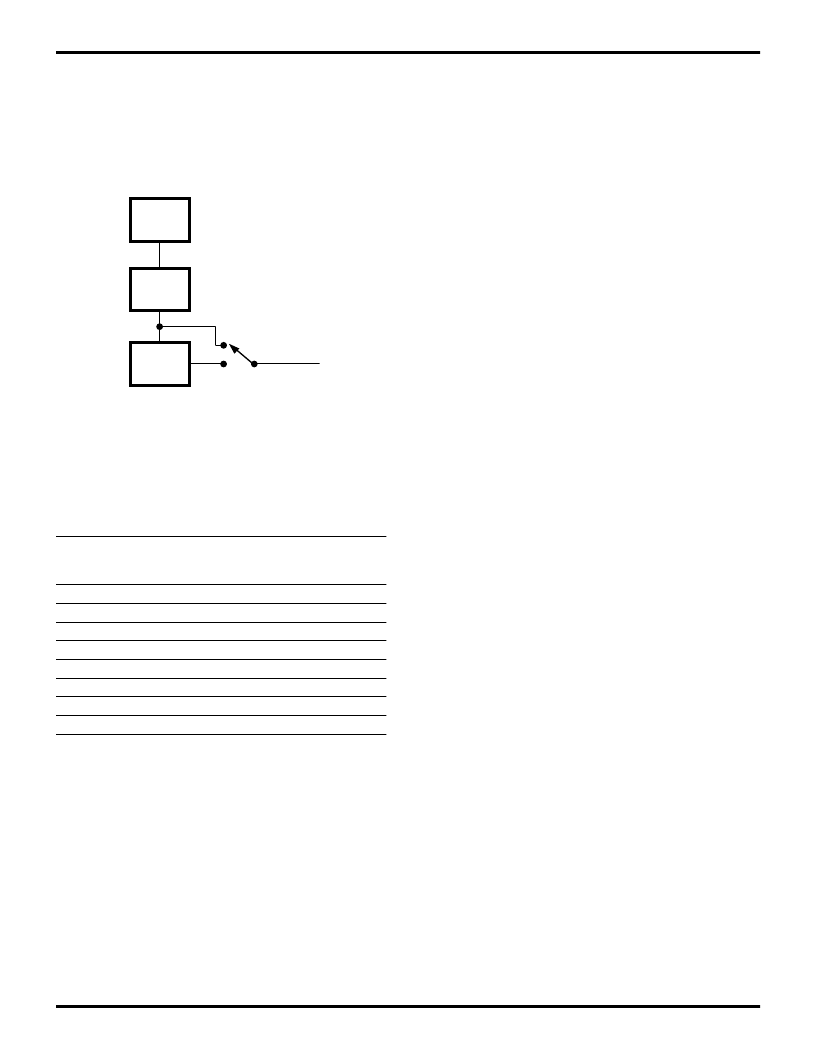
Figure 35. SCLK Circuit
Table 5. Stop-Mode Recovery Source
SMR:432
Operation
D4
0
0
0
0
1
1
1
1
D3
0
0
1
1
0
0
1
1
D2
0
1
0
1
0
1
0
1
Description of Action
POR and/or external reset recovery
Reserved
P31 transition
P32 transition
P33 transition
P27 transition
Logical NOR of P20 through P23
Logical NOR of P20 through P27
SMR, D0
÷
2
÷
16
OSC
SCLK
TCLK
相關(guān)PDF資料 |
PDF描述 |
|---|---|
| Z86C71 | IR/Low-Voltage Microcontroller |
| Z86L72 | IR MICROCONTROLLER |
| Z86C7216FSC | IR MICROCONTROLLER |
| Z86L7208FSC | IR MICROCONTROLLER |
| Z86L7208PSC | IR MICROCONTROLLER |
相關(guān)代理商/技術(shù)參數(shù) |
參數(shù)描述 |
|---|---|
| Z86L7608FSC | 制造商:未知廠家 制造商全稱:未知廠家 功能描述:8-Bit Microcontroller |
| Z86L7608PSC | 制造商:未知廠家 制造商全稱:未知廠家 功能描述:8-Bit Microcontroller |
| Z86L7608VSC | 制造商:未知廠家 制造商全稱:未知廠家 功能描述:8-Bit Microcontroller |
| Z86L7708FSC | 制造商:未知廠家 制造商全稱:未知廠家 功能描述:8-Bit Microcontroller |
| Z86L7708PSC | 制造商:未知廠家 制造商全稱:未知廠家 功能描述:8-Bit Microcontroller |
發(fā)布緊急采購,3分鐘左右您將得到回復。