- 您現(xiàn)在的位置:買賣IC網(wǎng) > PDF目錄373784 > ZL40518 (Zarlink Semiconductor Inc.) 3 Channel Laser Diode Driver PDF資料下載
參數(shù)資料
| 型號: | ZL40518 |
| 廠商: | Zarlink Semiconductor Inc. |
| 英文描述: | 3 Channel Laser Diode Driver |
| 中文描述: | 3通道激光二極管驅動器 |
| 文件頁數(shù): | 2/16頁 |
| 文件大小: | 330K |
| 代理商: | ZL40518 |
ZL40518
Data Sheet
2
Zarlink Semiconductor Inc.
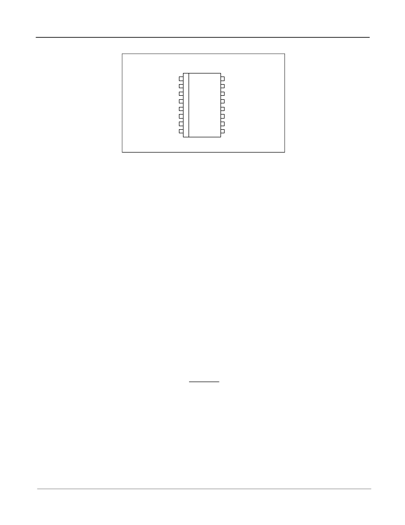
Figure 2 - Pinout of 16 Pin SSO16 Package (Top View)
Description
The ZL40518 is a laser diode driver for high speed operation of a grounded laser diode. The driver consists of 3
controllable channels: a switchable, low noise, read channel and two switchable write channels. Write current
pulses are enabled with the application of a low signal on the /EN pins. A summed output of all channels is
available at the IOUT pin. Each channel can contribute up to 250 mA to the total output current of up to 300 mA. A
total read channel gain of 100 and write channels 2 and 3 with a gain of 250 and 150 respectively are provided
between each reference current input and output.
Laser mode hopping noise during read mode can be reduced by the use of an on-chip RF oscillator. The oscillator
frequency and swing can be set by two external resistors. The oscillator is enabled by a high signal on the OSCEN
pin and the entire device can be switched off by the application of a low signal on the PWR_UP pin.
Application Notes
Read and Write Channel Operation
The read channel is activated by applying a 'High' signal to the PWR_UP pin and applying a 'low' signal to /ENR. In
this mode, the fast write channels can be enabled by applying a 'Low signal to the respective pair of write enable
pins (/EN2) or (/EN3). The output currents of the three channels are summed together and output as a composite
signal at IOUT.
Voltage control of the channel reference inputs (INR, IN2 and IN3) can be achieved quite easily using an external
resistor R
ref
in series with the reference channel input to convert a given reference potential V
ref
to an input current,
I
in
:
where R
in
is the input impedance of the respective reference channel.
On-Chip RF Oscillator
An on-chip RF oscillator is enabled if OSCEN = 'High', and its output signal is added to the current output.The
oscillator amplitude is set by an external resistor from RS to GND. Its frequency is set by an external resistor RF to
GND. The oscillator signal is summed with the programmed Write and Read levels before amplification to the
output. The oscillator signal has zero DC level and +I_pk to -I_pk signal swing. Consequently, if the programmed
DC level from the Write and Read Channels is less than the PK level programmed for the Oscillator, the combined
INR
IN2
GND
RF
IN3
/ENR
/EN3
VCC_IN
VCC
IOUT
GND
RS
PWR_UP
OSCEN
VCC
1
2
3
4
5
12
11
13
6
7
8
10
9
14
15
16
in
ref
ref
+
in
R
R
V
I
=
,
相關PDF資料 |
PDF描述 |
|---|---|
| ZL40518LDG | 3 Channel Laser Diode Driver |
| ZL40518DGE1 | 3 Channel Laser Diode Driver |
| ZL40539 | Dual Output CD and DVD 4 Channel Laser Diode Driver |
| ZL40539LCF | Dual Output CD and DVD 4 Channel Laser Diode Driver |
| ZL40539LCG | Dual Output CD and DVD 4 Channel Laser Diode Driver |
相關代理商/技術參數(shù) |
參數(shù)描述 |
|---|---|
| ZL40518DGE1 | 制造商:ZARLINK 制造商全稱:Zarlink Semiconductor Inc 功能描述:3 Channel Laser Diode Driver |
| ZL40518LDG | 制造商:ZARLINK 制造商全稱:Zarlink Semiconductor Inc 功能描述:3 Channel Laser Diode Driver |
| ZL40539 | 制造商:ZARLINK 制造商全稱:Zarlink Semiconductor Inc 功能描述:Dual Output CD and DVD 4 Channel Laser Diode Driver |
| ZL40539LCF | 制造商:Microsemi Corporation 功能描述: 制造商:Microsemi Corporation 功能描述:LASER DRVR 4-CH 32QFN - Trays |
| ZL40539LCG | 制造商:Microsemi Corporation 功能描述: 制造商:Microsemi Corporation 功能描述:4 CHAN LVDS LDD C3C31C - Trays 制造商:Rochester Electronics LLC 功能描述: 制造商:Zarlink Semiconductor Inc 功能描述: 制造商:ZARLINK 功能描述: |
發(fā)布緊急采購,3分鐘左右您將得到回復。