- 您現(xiàn)在的位置:買賣IC網(wǎng) > PDF目錄372977 > ZN447J Converter IC PDF資料下載
參數(shù)資料
| 型號(hào): | ZN447J |
| 英文描述: | Converter IC |
| 中文描述: | 轉(zhuǎn)換器IC |
| 文件頁(yè)數(shù): | 1/18頁(yè) |
| 文件大?。?/td> | 289K |
| 代理商: | ZN447J |
當(dāng)前第1頁(yè)第2頁(yè)第3頁(yè)第4頁(yè)第5頁(yè)第6頁(yè)第7頁(yè)第8頁(yè)第9頁(yè)第10頁(yè)第11頁(yè)第12頁(yè)第13頁(yè)第14頁(yè)第15頁(yè)第16頁(yè)第17頁(yè)第18頁(yè)
WR (START CONVERSION)
BUSY (END OF CONVERSION)
DB
0
(LSB)
RD (OUTPUT ENABLE)
DB
1
CLOCK
DB
2
DB
3
R
EXT
DB
4
V
IN
DB
5
V
REF
IN
DB
6
V
REF
OUT
DB
7
(MSB)
GROUND
+V
CC
(+5V)
18
1
17
2
16
3
15
4
14
5
13
6
12
7
11
8
10
9
WR (START CONVERSION)
BUSY (END OF CONVERSION)
DB
0
(LSB)
RD (OUTPUT ENABLE)
DB
1
CLOCK
DB
2
DB
3
R
EXT
DB
4
V
IN
DB
5
V
REF
IN
DB
6
V
REF
OUT
DB
7
(MSB)
GROUND
+V
CC
(+5V)
18
1
17
2
16
3
15
4
14
5
13
6
12
7
11
8
10
9
0
°
C to +70
°
C
0
°
C to +70
°
C
0
°
C to +70
°
C
0.5
1
1
ZN448/ZN449
8-BIT MICROPROCESSOR COMPATIBLE A-D CONVERTER
DS3013 - 2.2
The ZN448 and ZN449 are 8-bit successive
approximation A-D converters designed to be easily
interfaced to microprocessors. All active circuitry is contained
on-chip including a clock generator and stable 2.5V bandgap
reference, control logic and double buffered latches with
reference.
Only a reference resistor and capacitor, clock resistor and
capacitor and input resistors are required for operation with
either unipolar or bipolar input voltage.
FEATURES
I
Easy Interfacing to Microprocessor, or operates as a
'Stand-Alone' Converter
I
Fast: 9 microseconds Conversion time Guaranteed
I
Choice of Linearity: 0.5 LSB - ZN448, 1 LSB - ZN449
I
On-Chip Clock
I
Choice of On-Chip or External Reference Voltage
I
Unipolar or Bipolar Input Ranges
I
Commercial Temperature Range
ORDERING INFORMATION
Device type
ZN448E
ZN449D
ZN449E
Package
DP18
MP18
DP18
Operating
temperature
Linearity
error (LSB)
ZN448/9E (DP18)
ZN449D (MP18)
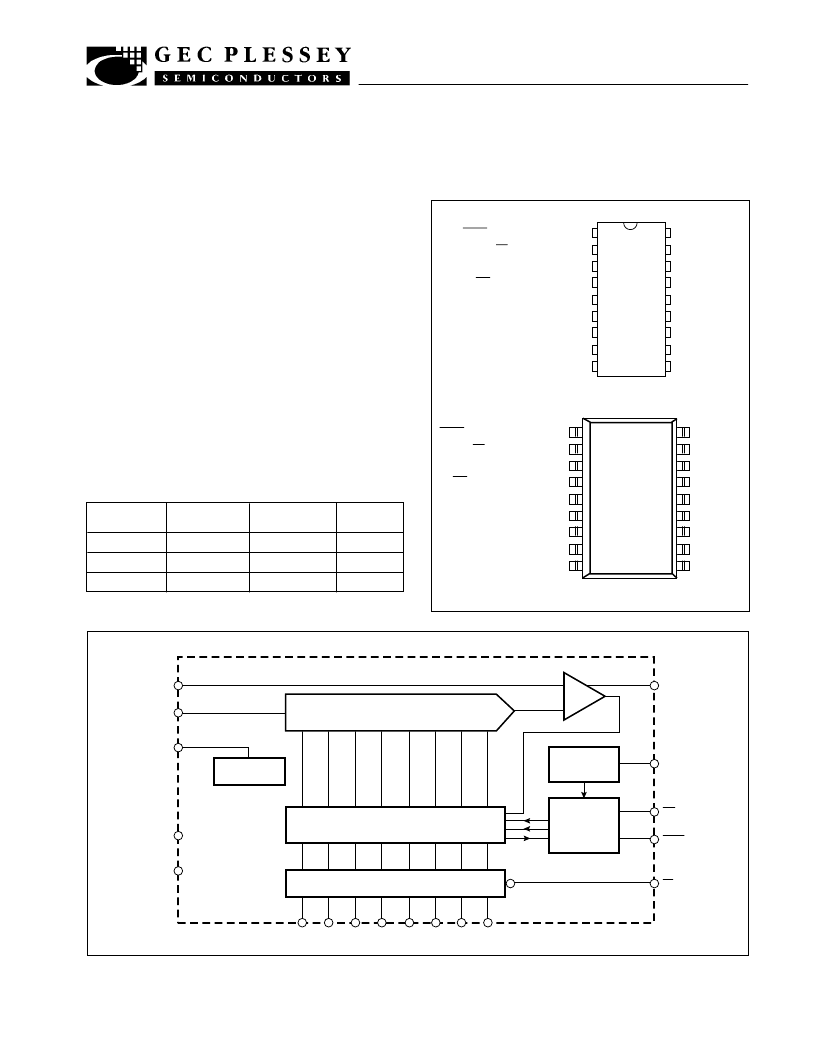
Fig.1 Pin connection - top view
Fig.2 System diagram
SUCCESSIVE
APPROXIMATION REGISTER
3-STATE BUFFERS
8-BIT DAC
2.5V
REFERENCE
CLOCK
GENERATOR
INTERFACE
AND
CONTROL
LOGIC
+
-
CK RC OR
EXT CLOCK
3
REXT
5
WR
4
BUSY
1
RD
2
18
17
16
15
14
13
12
DB0
11
DB7
VCC (+5V)
10
GROUND
9
VREF OUT
8
VREF IN
7
ANALOGUE
INPUT
6
COMPARATOR
相關(guān)PDF資料 |
PDF描述 |
|---|---|
| ZN448D | Converter IC |
| ZN448J | Converter IC |
| ZN449J | Converter IC |
| ZN448E | TV 53C 40#22D 9#16 4#12 PIN RE |
| ZN449 | TV 53C 40#22D 9#16 4#12 PIN RE |
相關(guān)代理商/技術(shù)參數(shù) |
參數(shù)描述 |
|---|---|
| ZN448 | 制造商:未知廠家 制造商全稱:未知廠家 功能描述:8-BIT MICROPROCESSOR COMPATIBLE A-D CONVERTER |
| ZN448D | 制造商:未知廠家 制造商全稱:未知廠家 功能描述:Converter IC |
| ZN448E | 制造商:GPS 功能描述: |
| ZN448J | 制造商:未知廠家 制造商全稱:未知廠家 功能描述:Converter IC |
| ZN449 | 制造商:未知廠家 制造商全稱:未知廠家 功能描述:8-BIT MICROPROCESSOR COMPATIBLE A-D CONVERTER |
發(fā)布緊急采購(gòu),3分鐘左右您將得到回復(fù)。