- 您現(xiàn)在的位置:買賣IC網(wǎng) > PDF目錄373840 > ZXCL260E5TA (ZETEX PLC) IC-SM-2.6V 150MA LDO REG PDF資料下載
參數(shù)資料
| 型號: | ZXCL260E5TA |
| 廠商: | ZETEX PLC |
| 元件分類: | 基準(zhǔn)電壓源/電流源 |
| 英文描述: | IC-SM-2.6V 150MA LDO REG |
| 中文描述: | 2.6 V FIXED POSITIVE LDO REGULATOR, 0.31 V DROPOUT, PDSO5 |
| 封裝: | SOT-23, 5 PIN |
| 文件頁數(shù): | 9/11頁 |
| 文件大小: | 374K |
| 代理商: | ZXCL260E5TA |
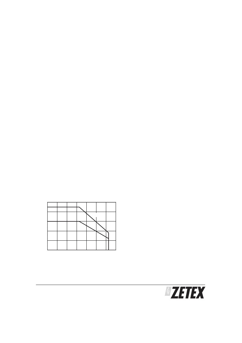
APPLICATIONS INFORMATION (Cont)
Power Dissipation
The maximum allowable power dissipation of the
devicefornormaloperation(Pmax),isafunctionofthe
package junction to ambient thermal resistance (
θ
ja),
maximum junction temperature (Tjmax), and ambient
temperature (Tamb), according to the expression:
P
max
= (Tj
max
–
T
amb
) /
θ
ja
The maximum output current (I
max
) at a given value of
Input voltage (V
IN
) and output voltage (V
OUT
) is then
given by
I
max
= P
max
/ (V
IN
- V
OUT
)
The value of
θ
ja is strongly dependent upon the type of
PC board used. Using the SC70 package it will range
fromapproximately280
°
C/Wforamulti-layerboardto
around 450
°
C/W for a single sided board. It will range
from 180
°
C/W to 300
°
C/W for the SOT23-5 package. To
avoid entering the thermal shutdown state, Tj
max
should be assumed to be 125
°
C and I
max
less than the
over-current limit,(I
OLIM
). Power derating for the SC70
and SOT23-5 packages is shown in the following
graph.
CapacitorSelectionandRegulatorStability
The device is designed to operate with all types of
output capacitor, including tantalum and low ESR
ceramic.Forstabilityoverthefulloperatingrangefrom
no load to maximum load, an output capacitor with a
minimum value of 1
μ
F is recommended, although this
can be increased without limit to improve load
transient performance. Higher values of output
capacitorwillalsoreduceoutputnoise.Capacitorswith
ESRlessthan0.5
arerecommendedforbestresults.
An input capacitor of 1
μ
F (ceramic or tantalum) is
recommended to filter supply noise at the device input
and will improve ripple rejection.
The input and output capacitors should be positioned
close to the device, and a ground plane board layout
shouldbeusedtominimisetheeffectsofparasitictrack
resistance.
Dropout Voltage
The output pass transistor is a large PMOS device,
which acts like a resistor when the regulator enters the
dropout region. The dropout voltage is therefore
proportional to output current as shown in the typical
characteristics.
Ground Current
The use of a PMOS device ensures a low value of
ground current under all conditions including dropout,
start-up and maximum load.
Power Supply Rejection and Load
Transient Response
Line and Load transient response graphs are shown in
the typical characteristics.
These show both the DC and dynamic shift in the
output voltage with step changes of input voltage and
load current, and how this is affected by the output
capacitor.
If improved transient response is required, then an
output capacitor with lower ESR value should be used.
Larger capacitors will reduce over/undershoot, but will
increase the settling time. Best results are obtained
using a ground plane layout to minimise board
parasitics.
ZXCL250 ZXCL260 ZXCL280
ZXCL300 ZXCL330 ZXCL400
9
-40
-20
0
Temperature (
°
C)
20
40
60
80
100
0
100
200
300
400
500
SOT23
SC70
Derating Curve
M
ISSUE 5 - NOVEMBER 2001
相關(guān)PDF資料 |
PDF描述 |
|---|---|
| ZXCL330 | Cap-Free, NMOS, 150mA Low Dropout Regulator with Reverse Current Protection |
| ZXCL330E5 | Cap-Free, NMOS, 150mA Low Dropout Regulator with Reverse Current Protection |
| ZXCL330H5 | Cap-Free, NMOS, 150mA Low Dropout Regulator with Reverse Current Protection |
| ZXCL400 | Cap-Free, NMOS, 150mA Low Dropout Regulator with Reverse Current Protection |
| ZXCL400E5 | Cap-Free, NMOS, 150mA Low Dropout Regulator with Reverse Current Protection |
相關(guān)代理商/技術(shù)參數(shù) |
參數(shù)描述 |
|---|---|
| ZXCL260E5TA | 制造商:Diodes Incorporated 功能描述:V REG LDO +2.6V SOT-23-5-5 260 |
| ZXCL260H5 | 制造商:ZETEX 制造商全稱:ZETEX 功能描述:ULTRA SMALL MICROPOWER SC70 LOW DROPOUT REGULATORS |
| ZXCL260H5TA | 功能描述:低壓差穩(wěn)壓器 - LDO 2.6V 150mA Sgl LDO RoHS:否 制造商:Texas Instruments 最大輸入電壓:36 V 輸出電壓:1.4 V to 20.5 V 回動電壓(最大值):307 mV 輸出電流:1 A 負(fù)載調(diào)節(jié):0.3 % 輸出端數(shù)量: 輸出類型:Fixed 最大工作溫度:+ 125 C 安裝風(fēng)格:SMD/SMT 封裝 / 箱體:VQFN-20 |
| ZXCL280 | 制造商:ZETEX 制造商全稱:ZETEX 功能描述:ULTRA SMALL MICROPOWER SC70 LOW DROPOUT REGULATORS |
| ZXCL280E5 | 制造商:ZETEX 制造商全稱:ZETEX 功能描述:MICROPOWER SC70-5 & SOT23-5 LOW DROPOUT REGULATORS |
發(fā)布緊急采購,3分鐘左右您將得到回復(fù)。