- 您現(xiàn)在的位置:買賣IC網(wǎng) > PDF目錄382783 > μPD703000 (NEC Corp.) 16/32 Bit Single Chip Microcontrollers(16/32位單片微控制器) PDF資料下載
參數(shù)資料
| 型號: | μPD703000 |
| 廠商: | NEC Corp. |
| 英文描述: | 16/32 Bit Single Chip Microcontrollers(16/32位單片微控制器) |
| 中文描述: | 16/32位單片機(jī)微控制器(16/32位單片微控制器) |
| 文件頁數(shù): | 46/88頁 |
| 文件大?。?/td> | 614K |
| 代理商: | ΜPD703000 |
第1頁第2頁第3頁第4頁第5頁第6頁第7頁第8頁第9頁第10頁第11頁第12頁第13頁第14頁第15頁第16頁第17頁第18頁第19頁第20頁第21頁第22頁第23頁第24頁第25頁第26頁第27頁第28頁第29頁第30頁第31頁第32頁第33頁第34頁第35頁第36頁第37頁第38頁第39頁第40頁第41頁第42頁第43頁第44頁第45頁當(dāng)前第46頁第47頁第48頁第49頁第50頁第51頁第52頁第53頁第54頁第55頁第56頁第57頁第58頁第59頁第60頁第61頁第62頁第63頁第64頁第65頁第66頁第67頁第68頁第69頁第70頁第71頁第72頁第73頁第74頁第75頁第76頁第77頁第78頁第79頁第80頁第81頁第82頁第83頁第84頁第85頁第86頁第87頁第88頁
46
μ
PD703000, 703001
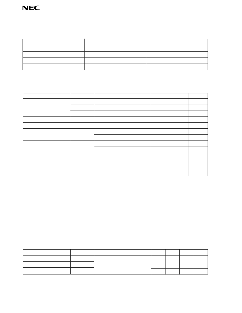
12. ELECTRICAL SPECIFICATIONS
Supported Electrical Characteristics
Part Number
V
DD
= 5.0 V
±
10%
V
DD
= 3.0 to 3.6 V
μ
PD703000GC-25-xxx-7EA
Electrical characteristics specified
Outside of guaranteed operating range
μ
PD703001GC-25-7EA
Electrical characteristics specified
Outside of guaranteed operating range
μ
PD703000GC-33-xxx-7EA
Electrical characteristics specified
Electrical characteristics specified
μ
PD703001GC-33-7EA
Electrical characteristics specified
Electrical characteristics specified
Remark
xxx indicates a ROM code suffix.
12.1 When V
DD
= 5.0 V
±
10%
Absolute Maximum Ratings (T
A
= 25
°
C)
Parameter
Symbol
Condition
Rating
Unit
Supply voltage
V
DD
V
DD
pin
–0.5 to +7.0
V
CV
DD
CV
DD
pin
–0.5 to +7.0
V
CV
SS
CV
SS
pin
–0.5 to +0.5
V
Input voltage
V
I1
Except X1 pin, V
DD
= 5.0 V
±
10%
–0.5 to V
DD
+0.3
V
Clock input voltage
Vx
X1 pin, V
DD
= 5.0
±
10%
–0.5 to V
DD
+1.0
V
Output current, low
I
OL
1 pin
4.0
mA
Total of all pins
100
mA
Output current, high
I
OH
1 pin
–4.0
mA
Total of all pins
–100
mA
Output voltage
V
O
V
DD
= 5.0 V
±
10%
–0.5 to V
DD
+0.3
V
Operating temperature
T
A
Operating at 25 MHz
–40 to +85
°
C
Operating at 33 MHz
–20 to +70
°
C
Storage temperature
T
stg
–65 to +150
°
C
Cautions 1.
Do not directly connect to the output (or I/O) pins of an IC product, or to the V
DD
, V
CC
, or
GND.
Open-drain pins and open-collector pins may be connected each other however. Moreover,
an external circuit that is designed so as to avoid output contention can be directly
connected to a pin that goes into a high-impedance state.
If even one of the parameters exceeds the absolute maximum ratings even momentarily,
the quality of the product may be impaired. The absolute maximum ratings specify the
values exceeding which the product may be physically damaged. Never exceed these
ratings when using the products.
The specifications and conditions shown in DC and AC Characteristics below specify the
range in which the product operates normally and the product quality is guaranteed.
2.
Capacitance (T
A
= 25
°
C, V
DD
= V
SS
= 0 V)
Parameter
Symbol
Condition
MIN.
TYP.
MAX.
Unit
Input capacitance
C
I
f
C
= 1 MHz
15
pF
I/O capacitance
C
IO
0 V for pins other than test pin
15
pF
Output capacitance
C
O
15
pF
相關(guān)PDF資料 |
PDF描述 |
|---|---|
| μPD703001 | 16/32 Bit Single Chip Microcontrollers(16/32位單片微控制器) |
| μPD703008YGJ-33-8EU | 32 Bit RISC Microcontrollers(32位RISC微控制器) |
| μPD70F3008YGJ-33-8EU | 32 Bit RISC Microcontrollers(32位RISC微控制器) |
| μPD703015 | 8/16 Bit Single Chip Microcontrollers(8/16位單片微控制器) |
| μPD703015Y | 8/16 Bit Single Chip Microcontrollers(8/16位單片微控制器) |
相關(guān)代理商/技術(shù)參數(shù) |
參數(shù)描述 |
|---|---|
| PD7035 | 制造商:MITSUBISHI 制造商全稱:Mitsubishi Electric Semiconductor 功能描述:FOR OPTICAL COMMUNICATION |
| PD7087 | 制造商:MITSUBISHI 制造商全稱:Mitsubishi Electric Semiconductor 功能描述:InGaAs PIN PHOTO DIODES |
| PD7088 | 制造商:MITSUBISHI 制造商全稱:Mitsubishi Electric Semiconductor 功能描述:InGaAs PIN PHOTO DIODES |
| PD708C7 | 制造商:MITSUBISHI 制造商全稱:Mitsubishi Electric Semiconductor 功能描述:InGaAs PIN PHOTO DIODES |
| PD708C8 | 制造商:MITSUBISHI 制造商全稱:Mitsubishi Electric Semiconductor 功能描述:InGaAs PIN PHOTO DIODES |
發(fā)布緊急采購,3分鐘左右您將得到回復(fù)。