- 您現(xiàn)在的位置:買(mǎi)賣(mài)IC網(wǎng) > PDF目錄371394 > 24C01C-IST (Microchip Technology Inc.) IC, QUAD PHY 10GX PDF資料下載
參數(shù)資料
| 型號(hào): | 24C01C-IST |
| 廠商: | Microchip Technology Inc. |
| 英文描述: | IC, QUAD PHY 10GX |
| 中文描述: | 一千5.0VI 2葷⑩串行EEPROM |
| 文件頁(yè)數(shù): | 6/12頁(yè) |
| 文件大?。?/td> | 326K |
| 代理商: | 24C01C-IST |

24C01C
DS21201A-page 6
Preliminary
1997 Microchip Technology Inc.
5.0
DEVICE ADDRESSING
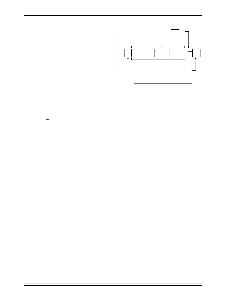
A control byte is the first byte received following the
start condition from the master device (Figure 5-1). The
control byte consists of a four bit control code; for the
24C01C this is set as 1010 binary for read and write
operations. The next three bits of the control byte are
the chip select bits (A2, A1, A0). The chip select bits
allow the use of up to eight 24C01C devices on the
same bus and are used to select which device is
accessed. The chip select bits in the control byte must
correspond to the logic levels on the corresponding A2,
A1, and A0 pins for the device to respond. These bits
are in effect the three most significant bits of the word
address.
The last bit of the control byte defines the operation to
be performed. When set to a one a read operation is
selected, and when set to a zero a write operation is
selected. Following the start condition, the 24C01C
monitors the SDA bus checking the control byte being
transmitted. Upon receiving a 1010 code and appropri-
ate chip select bits, the slave device outputs an
acknowledge signal on the SDA line. Depending on the
state of the R/W bit, the 24C01C will select a read or
write operation.
FIGURE 5-1:
CONTROL BYTE FORMAT
Read/Write Bit
5.1
Contiguous Addressing Across
Multiple Devices
The chip select bits A2, A1, A0 can be used to expand
the contiguous address space for up to 8K bits by add-
ing up to eight 24C01C devices on the same bus. In this
case, software can use A0 of the control byte as
address bit A8, A1 as address bit A9, and A2 as
address bit A10. It is not possible to write or read across
device boundaries.
1
0
1
0
A2
A1
A0
S
ACK
R/W
Control Code
Chip Select
Bits
Slave Address
Acknowledge Bit
Start Bit
相關(guān)PDF資料 |
PDF描述 |
|---|---|
| 24C01C-P | 1K 5.0V I 2 C ⑩ Serial EEPROM |
| 24C01C-SN | 1K 5.0V I 2 C ⑩ Serial EEPROM |
| 24C01C-ST | 1K 5.0V I 2 C ⑩ Serial EEPROM |
| 24C01C-EP | 71-255612-08P |
| 24C01C-ESN | PTSE 8C 8#20 STR PLUG |
相關(guān)代理商/技術(shù)參數(shù) |
參數(shù)描述 |
|---|---|
| 24C01CP | 制造商:Microchip Technology Inc 功能描述: |
| 24C01C-P | 制造商:MICROCHIP 制造商全稱:Microchip Technology 功能描述:1K 5.0V I 2 C ⑩ Serial EEPROM |
| 24C01CSN | 制造商:Microchip Technology Inc 功能描述: |
| 24C01C-SN | 制造商:MICROCHIP 制造商全稱:Microchip Technology 功能描述:1K 5.0V I 2 C ⑩ Serial EEPROM |
| 24C01C-ST | 制造商:MICROCHIP 制造商全稱:Microchip Technology 功能描述:1K 5.0V I 2 C ⑩ Serial EEPROM |
發(fā)布緊急采購(gòu),3分鐘左右您將得到回復(fù)。