- 您現(xiàn)在的位置:買賣IC網(wǎng) > PDF目錄371396 > 24LC515 (Microchip Technology Inc.) 512K I2C CMOS Serial EEPROM PDF資料下載
參數(shù)資料
| 型號: | 24LC515 |
| 廠商: | Microchip Technology Inc. |
| 英文描述: | 512K I2C CMOS Serial EEPROM |
| 中文描述: | 為512k的I2C的CMOS串行EEPROM |
| 文件頁數(shù): | 7/22頁 |
| 文件大?。?/td> | 285K |
| 代理商: | 24LC515 |

2003 Microchip Technology Inc.
Preliminary
DS21673C-page 7
24AA515/24LC515/24FC515
5.0
DEVICE ADDRESSING
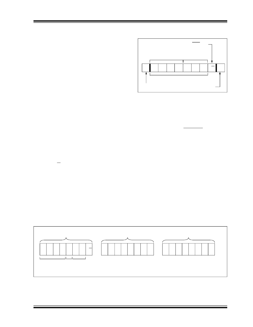
A control byte is the first byte received following the
Start condition from the master device (Figure 5-1).
The control byte consists of a 4-bit control code; for the
24XX515, this is set as ‘
1010
’ binary for read and write
operations. The next bit of the control byte is the block
select bit (B0). This bit acts as the A15 address bit for
accessing the entire array. The next two bits of the
control byte are the Chip Select bits (A1, A0). The Chip
Select bits allow the use of up to four 24XX515 devices
on the same bus and are used to select which device is
accessed. The Chip Select bits in the control byte must
correspond to the logic levels on the corresponding A1
and A0 pins for the device to respond. These bits are in
effect the two Most Significant bits of the word address.
The last bit of the control byte defines the operation to
be performed. When set to a one, a read operation is
selected, and when set to a zero, a write operation is
selected. The next two bytes received define the
address of the first data byte (Figure 5-2). Because
only A14…A0 are used, the upper address bit is a don’t
care. The upper address bits are transferred first,
followed by the less significant bits.
Following the Start condition, the 24XX515 monitors
the SDA bus checking the device type identifier being
transmitted. Upon receiving a ‘
1010
’ code and appro-
priate device select bits, the slave device outputs an
Acknowledge signal on the SDA line. Depending on the
state of the R/W bit, the 24XX515 will select a read or
write operation.
This device has an internal addressing boundary
limitation that is divided into two segments of 256K bits.
Block select bit ‘B0’ is used in place of address bit
location ‘A15’ to control access to each segment.
FIGURE 5-1:
CONTROL BYTE
FORMAT
5.1
Contiguous Addressing Across
Multiple Devices
The Chip Select bits A1, A0 can be used to expand the
contiguous address space for up to 2 Mbit by adding up
to four 24XX515's on the same bus. In this case,
software can use A0 of the control byte as address bit
A16 and A1 as address bit A17. It is not possible to
sequentially read across device boundaries.
Each device has internal addressing boundary
limitations. This divides each part into two segments of
256K bits. The block select bit ‘B0’ controls access to
each “half” rather than address bit location A15.
Sequential read operations are limited to 256K blocks.
To read through four devices on the same bus, eight
random Read commands must be given.
FIGURE 5-2:
ADDRESS SEQUENCE BIT ASSIGNMENTS
1
0
1
0
B0
A1
A0
S
ACK
R/W
Control Code
Chip Select
Bits
Slave Address
Acknowledge Bit
Start Bit
Read/Write Bit
1
0
1
0
B
0
A
1
A
X
A
11
A
10
A
9
A
7
A
0
A
8
A
12
CONTROL BYTE
ADDRESS HIGH BYTE
ADDRESS LOW BYTE
CONTROL
CODE
CHIP
SELECT
BITS
X = Don’t Care Bit
A
13
A
14
BLOCK
SELECT
BIT
相關PDF資料 |
PDF描述 |
|---|---|
| 24FC65-IP | 64K 5.0V 1 MHz I 2 C Smart Serial EEPROM |
| 24FC65-ISM | 64K 5.0V 1 MHz I 2 C Smart Serial EEPROM |
| 24FC65-P | 64K 5.0V 1 MHz I 2 C Smart Serial EEPROM |
| 24FC65-SM | 64K 5.0V 1 MHz I 2 C Smart Serial EEPROM |
| 24FC65 | 64K 5.0V 1MHz CMOS Smart Serial EEPROMs(4.5~5.5V,64K位,10M次擦寫周期,IIC智能串行EEPROM) |
相關代理商/技術參數(shù) |
參數(shù)描述 |
|---|---|
| 24LC515-I/P | 功能描述:電可擦除可編程只讀存儲器 64kx8 64B - 2.5V RoHS:否 制造商:Atmel 存儲容量:2 Kbit 組織:256 B x 8 數(shù)據(jù)保留:100 yr 最大時鐘頻率:1000 KHz 最大工作電流:6 uA 工作電源電壓:1.7 V to 5.5 V 最大工作溫度:+ 85 C 安裝風格:SMD/SMT 封裝 / 箱體:SOIC-8 |
| 24LC515-I/P | 制造商:Microchip Technology Inc 功能描述:IC EEPROM SERIAL 512K |
| 24LC515-I/SM | 功能描述:電可擦除可編程只讀存儲器 64kx8 64B - 2.5V RoHS:否 制造商:Atmel 存儲容量:2 Kbit 組織:256 B x 8 數(shù)據(jù)保留:100 yr 最大時鐘頻率:1000 KHz 最大工作電流:6 uA 工作電源電壓:1.7 V to 5.5 V 最大工作溫度:+ 85 C 安裝風格:SMD/SMT 封裝 / 箱體:SOIC-8 |
| 24LC515-I/SM | 制造商:Microchip Technology Inc 功能描述:EEPROM SERIAL 512K 64B PAGE SMD |
| 24LC515ISM | 制造商:Microchip Technology Inc 功能描述: |
發(fā)布緊急采購,3分鐘左右您將得到回復。