- 您現(xiàn)在的位置:買賣IC網(wǎng) > PDF目錄371415 > 27174A Versatile I/0: DQ--VI/O and Enhanced--VI/O PDF資料下載
參數(shù)資料
| 型號: | 27174A |
| 英文描述: | Versatile I/0: DQ--VI/O and Enhanced--VI/O |
| 中文描述: | 通用的I / 0:宿舍-六/ O和增強-六/輸出 |
| 文件頁數(shù): | 2/4頁 |
| 文件大?。?/td> | 67K |
| 代理商: | 27174A |

Publication#
27174
Issue Date:
October 23, 2002
Rev:
A
Amendment/
0
Versatile I/O: DQ
–
V
I/O
and Enhanced
–
V
I/O
Application Note
This document describes the two types of Versatile I/O
provided by AMD Flash memory: DQ-V
I/O
and En-
hanced-V
I/O
. Also described are the benefits of
designing with AMD’s Versatile I/O Flash memory in
terms of reducing system complexity, and the limita-
tions of each type of Versatile I/O interface.
What is Versatile I/O (V
I/O
)
Versatile I/O (V
I/O
) is used on AMD Flash memory to
provide support for I/O signaling that is outside the
“normal” operating range of a device. Versatile I/O al-
lows a 3.0V AMD Flash to be compatible with 2.5V or
1.8V devices without the need of expensive voltage
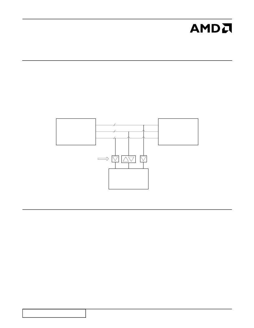
translation buffers, as shown in Figure 1. Also, Versa-
tile I/O enables this without affecting the overall
performance of the Flash device.
Figure 1.
I/O Signaling to Typical 3V Flash
Versatile I/O devices can provide this internal voltage
conversion because unlike traditional Flash memory,
where a single power supply (V
CC
) is used to power
both the memory array and I/O pins, V
CC
only powers
the memory array while the V
I/O
pin(s) power the I/O
pins. This allows a Versatile I/O Flash device to directly
interface with a wide variety of FPGAs, ASICs, micro-
processors, microcontrollers, and other digital devices
regardless of the device operating voltage. For exam-
ple if a board is using a 3.0V AMD Flash, and a 1.8V
microcontroller. A typical Flash would have problems
since the typical minimum legal high for a 3.0V device
is 2.1V (3.0V * 0.7 = 2.1V), this is higher than the
source voltage of the 1.8V microcontroller. With AMD’s
Versatile I/O Flash memory the V
I/O
pin(s) would be
connected to the 1.8V source used by the microcontrol-
ler, making the voltage levels for the inputs and outputs
JEDEC 1.8V compliant.
System Performance
The performance of the system shown in Figure 1 is
also greatly affected because of the need for transla-
tion buffers. The buffers consume up to 100 mA of
current each and data skew will occur any time a signal
passes through the buffers. This data skew is due to vari-
ations in the propagation delay between parts and also
between the individual pins on a buffer. However, the
skew between individual pins is typically much smaller
than between individual buffer chips.
The propagation delays through voltage translation
buffers are highly variable, on the order of 2 ns to 7 ns,
and discrepant on bi-directional buffers. In Figure 1,
MicroController
Vcc = 1.8v
Address
Data
Control
x8
x16
x24
Typical 3v
Flash
Other 1.8v
Devices
32
16
8
Voltage
Translation
Buffers
相關(guān)PDF資料 |
PDF描述 |
|---|---|
| 2718BD2 | Upo Interface Xfmr |
| 2718BG2 | Upo Interface Xfmr |
| 271KD25NX | 130 to 1000 Volts Varistor 155 to 1100 Joule |
| 271P25.28.F | ±15kV ESD-Protected USB Level Translators in UCSP |
| 279P25.28.F | 2.7Gbps, Low-Power SFP Laser Drivers |
相關(guān)代理商/技術(shù)參數(shù) |
參數(shù)描述 |
|---|---|
| 271-75 | 功能描述:金屬膜電阻器 - 透孔 75ohms 1% 50PPM RoHS:否 制造商:IRC 電阻:63.4 kOhms 容差:1 % 功率額定值:100 mW 電壓額定值:200 V 溫度系數(shù):100 PPM / C 端接類型:Axial 工作溫度范圍: 尺寸:2.3 mm Dia. x 6.4 mm L 封裝:Bulk |
| 271-75.5/AP | 功能描述:金屬膜電阻器 - 透孔 USE 271-75.5/AP-RC 50PPM RoHS:否 制造商:IRC 電阻:63.4 kOhms 容差:1 % 功率額定值:100 mW 電壓額定值:200 V 溫度系數(shù):100 PPM / C 端接類型:Axial 工作溫度范圍: 尺寸:2.3 mm Dia. x 6.4 mm L 封裝:Bulk |
| 271-75.5/AP-RC | 功能描述:金屬膜電阻器 - 透孔 75.5ohms 1% 50PPM RoHS:否 制造商:IRC 電阻:63.4 kOhms 容差:1 % 功率額定值:100 mW 電壓額定值:200 V 溫度系數(shù):100 PPM / C 端接類型:Axial 工作溫度范圍: 尺寸:2.3 mm Dia. x 6.4 mm L 封裝:Bulk |
| 271-75.5/REEL | 功能描述:金屬膜電阻器 - 透孔 75.5ohms 1% 50PPM RoHS:否 制造商:IRC 電阻:63.4 kOhms 容差:1 % 功率額定值:100 mW 電壓額定值:200 V 溫度系數(shù):100 PPM / C 端接類型:Axial 工作溫度范圍: 尺寸:2.3 mm Dia. x 6.4 mm L 封裝:Bulk |
| 271-75.5/REEL-RC | 功能描述:金屬膜電阻器 - 透孔 75.5ohms 1% 50PPM RoHS:否 制造商:IRC 電阻:63.4 kOhms 容差:1 % 功率額定值:100 mW 電壓額定值:200 V 溫度系數(shù):100 PPM / C 端接類型:Axial 工作溫度范圍: 尺寸:2.3 mm Dia. x 6.4 mm L 封裝:Bulk |
發(fā)布緊急采購,3分鐘左右您將得到回復(fù)。