- 您現(xiàn)在的位置:買賣IC網(wǎng) > PDF目錄30463 > 2N6661JTX02 (VISHAY SILICONIX) 860 mA, 90 V, N-CHANNEL, Si, SMALL SIGNAL, MOSFET, TO-205AD PDF資料下載
參數(shù)資料
| 型號(hào): | 2N6661JTX02 |
| 廠商: | VISHAY SILICONIX |
| 元件分類: | 小信號(hào)晶體管 |
| 英文描述: | 860 mA, 90 V, N-CHANNEL, Si, SMALL SIGNAL, MOSFET, TO-205AD |
| 封裝: | TO-39 TOLL LID, 3 PIN |
| 文件頁(yè)數(shù): | 2/6頁(yè) |
| 文件大小: | 124K |
| 代理商: | 2N6661JTX02 |
2N6661, 2N6661-2, 2N6661JANTX, 2N6661JANTXV
www.vishay.com
Vishay Siliconix
S11-1542-Rev. D, 01-Aug-11
2
Document Number: 70225
THIS DOCUMENT IS SUBJECT TO CHANGE WITHOUT NOTICE. THE PRODUCTS DESCRIBED HEREIN AND THIS DOCUMENT
ARE SUBJECT TO SPECIFIC DISCLAIMERS, SET FORTH AT www.vishay.com/doc?91000
Notes
a. FOR DESIGN AID ONLY, not subject to production testing.
b. Pulse test: PW
300 μs duty cycle 2 %.
c. Switching time is essentially independent of operating temperature.
d. This parameter not registered with JEDEC.
Stresses beyond those listed under “Absolute Maximum Ratings” may cause permanent damage to the device. These are stress ratings only, and functional operation
of the device at these or any other conditions beyond those indicated in the operational sections of the specifications is not implied. Exposure to absolute maximum
rating conditions for extended periods may affect device reliability.
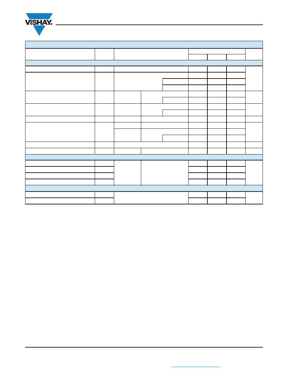
SPECIFICATIONS (TA = 25 °C, unless otherwise noted)
PARAMETER
SYMBOL
TEST CONDITIONS
LIMITS
UNIT
MIN.
TYP.b
MAX.
Static
Drain-Source Breakdown Voltage
VDS
VDS = 0 V, ID = 10 μA
90
125
-
V
Gate-Source Threshold Voltage
VGS(th)
VDS = VGS, ID = 1 mA
0.8
1.6
2
TA = - 55 °C
-1.8
2.5
TA = 125 °C
0.3
1.3
-
Gate-Body Leakage
IGSS
VGS = ± 20 V
VDS = 0 V
-
± 100
nA
TA = 125 °C
-
± 500
Zero Gate Voltage Drain Current
IDSS
VGS = 0 V
VDS = 72 V
--
1
μA
TA = 125 °C
-
100
On-State Drain Currentb
ID(on)
VGS = 10 V
VDS = 10 V
-1.8
-
mA
Drain-Source On-State Resistanceb
RDS(on)
VGS = 5 V
ID = 0.3 A
-3.8
5.3
VGS = 10 V
ID = 1 A
-3.6
4
TA = 125 °Cd
-6.7
7.5
Forward Transconductanceb
gfs
VDS = 7.5 V, ID = 0.475 A
170
340
-
mS
Diode Forward Voltage
VSD
VGS = 0 V
IS = 0.86 A
0.7
0.9
1.4
V
Dynamic
Input Capacitance
Ciss
VGS = 0 V
VDS = 25 V, f = 1 MHz
-35
50
pF
Output Capacitance
Coss
-15
40
Reverse Transfer Capacitance
Crss
-2
10
Drain-Source Capacitance
Cds
-30-
Switchingc
Turn-On Time
tON
VDD = 25 V, RL = 23
ID 1 A, VGEN = 10 V, Rg = 23
-6
10
ns
Turn-Off Time
tOFF
-8
10
相關(guān)PDF資料 |
PDF描述 |
|---|---|
| 2N6661JTXP02 | 860 mA, 90 V, N-CHANNEL, Si, SMALL SIGNAL, MOSFET, TO-205AD |
| 2N6661M1A | 1 A, 90 V, 4 ohm, N-CHANNEL, Si, POWER, MOSFET, TO-257AA |
| 2N6661 | 90 V, N-CHANNEL, Si, SMALL SIGNAL, MOSFET, TO-39 |
| 2N6667 | 10 A, 60 V, PNP, Si, POWER TRANSISTOR, TO-220AB |
| 2N6667 | 10 A, 60 V, PNP, Si, POWER TRANSISTOR, TO-220AB |
相關(guān)代理商/技術(shù)參數(shù) |
參數(shù)描述 |
|---|---|
| 2N6661JTXL02 | 制造商:Vishay Siliconix 功能描述:WITH SOLDER DIP WAIVERED PART - Bulk |
| 2N6661JTXP02 | 制造商:Vishay Siliconix 功能描述:WITH PN D WAIVERED PART - Bulk |
| 2N6661JTXV02 | 制造商:Vishay Angstrohm 功能描述:Trans MOSFET N-CH 90V 0.86A 3-Pin TO-205AD 制造商:Vishay Siliconix 功能描述:TRANS MOSFET N-CH 90V 0.9A 3PIN TO-205AD - Bulk |
| 2N6661M1A | 制造商:SEME-LAB 制造商全稱:Seme LAB 功能描述:N-CHANNEL ENHANCEMENT MODE POWER MOSFET |
| 2N6666 | 功能描述:兩極晶體管 - BJT PNP Pwr Darlington RoHS:否 制造商:STMicroelectronics 配置: 晶體管極性:PNP 集電極—基極電壓 VCBO: 集電極—發(fā)射極最大電壓 VCEO:- 40 V 發(fā)射極 - 基極電壓 VEBO:- 6 V 集電極—射極飽和電壓: 最大直流電集電極電流: 增益帶寬產(chǎn)品fT: 直流集電極/Base Gain hfe Min:100 A 最大工作溫度: 安裝風(fēng)格:SMD/SMT 封裝 / 箱體:PowerFLAT 2 x 2 |
發(fā)布緊急采購(gòu),3分鐘左右您將得到回復(fù)。