- 您現(xiàn)在的位置:買賣IC網(wǎng) > PDF目錄293797 > 3650MGHG Optically-Coupled Linear ISOLATION AMPLIFIERS PDF資料下載
參數(shù)資料
| 型號(hào): | 3650MGHG |
| 元件分類: | 隔離放大器 |
| 英文描述: | Optically-Coupled Linear ISOLATION AMPLIFIERS |
| 中文描述: | 光耦合線性隔離放大器 |
| 文件頁(yè)數(shù): | 10/13頁(yè) |
| 文件大?。?/td> | 127K |
| 代理商: | 3650MGHG |
第1頁(yè)第2頁(yè)第3頁(yè)第4頁(yè)第5頁(yè)第6頁(yè)第7頁(yè)第8頁(yè)第9頁(yè)當(dāng)前第10頁(yè)第11頁(yè)第12頁(yè)第13頁(yè)

6
3650/52
DEFINITIONS
ISOLATION-MODE VOLTAGE, VISO
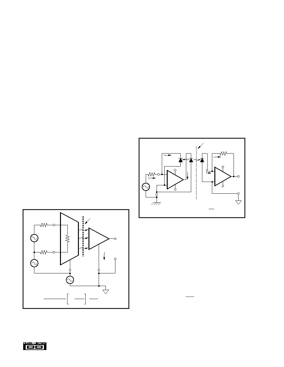
The isolation-mode voltage is the voltage which appears
across the isolation barrier, i.e., between the input common
and the output common. (See Figure 1.)
Two isolation voltages are given in the electrical specifica-
tions: “rated continuous” and “test voltage”. Since it is
impractical on a production basis to test a “continuous”
voltage (infinite test time is implied), it is a generally
accepted practice to test at a significantly higher voltage for
some reasonable length of time. For the 3650 and 3652, the
“test voltage” is equal to 1000V plus two times the “rated
continuous” voltage. Thus, for a continuous rating of 2000V,
each unit is tested at 5000V.
COMMON-MODE VOLTAGE, VCM
The common-mode voltage is the voltage midway between
the two inputs of the amplifier measured with respect to
input common. It is the algebraic average of the voltage
applied at the amplifiers’ input terminals. In the circuit in
Figure 1, (V+ + V–)/2 = VCM. (NOTE: Many applications
involve a large system “common-mode voltage.” Usually in
such cases the term defined here as “VCM” is negligible and
the system “common-mode voltage” is applied to the ampli-
fier as “VISO” in Figure 1.)
ISOLATION-MODE REJECTION
The isolation-mode rejection is defined by the equation in
Figure 1. The isolation-mode rejection is not infinite be-
cause there is some leakage across the isolation barrier due
to the isolation resistance and capacitance.
FIGURE 1. Illustration of Isolation-Mode and Common-
Mode Specifications.
NONLINEARITY
Nonlinearity is specified to be the peak deviation from a best
straightline expressed as a percent of peak-to-peak full scale
output (i.e.
±10mV at 20Vp-p ≈ 0.05%).
THEORY OF OPERATION
Prior to the introduction of the 3650 family optical isolation
had not been practical in linear circuits. A single LED and
photodiode combination, while useful in a wide range of
digital isolation applications, has fundamental limitations—
primarily nonlinearity and instability as a function of time
and temperature.
The 3650 and 3652 use a unique technique to overcome the
limitations of the single LED and photodiode isolator.
Figure 2 is an elementary equivalent circuit for the 3650,
which can be used to understand the basic operation without
considering the cluttering details of offset adjustment and
biasing for bipolar operation.
FIGURE 2. Simplified Equivalent Circuit of Linear Isolator.
Two matched photodiodes are used—one in the input (CR3)
and one in the output stage (CR2)—to greatly reduce
nonlinearities and time-temperature instabilities. Amplifier
A1, LED CR1, and photodiode CR3 are used in a negative
feedback configuration such that I1 = IIN RG (where RG is the
user supplied gain setting resistor). Since CR2 and CR3 are
closely matched, and since they receive equal amounts of
light from the LED CR1 (i.e., λ1 = λ2), I2 = I1 = IIN. Amplifier
A2 is connected as a current-to-voltage converter with VOUT
= I2 RK where RK is an internal 1M scaling resistor. Thus
the overall transfer function is:
VOUT = VIN
, (RG in s)
This improved isolator circuit overcomes the primary
limitations of the single LED and photodiode combination.
The transfer function is now virtually independent of any
degradation in the LED output as long as the two photo-
diodes and optics are closely matched(1). Linearity is now a
NOTE: (1) The only effect of decreased LED output is a slight decrease in full
scale swing capability. See Typical Performance Curves.
C
(Output)
+
R
G1
R
G2
R
IN
V
ISO
V
CM
V
D
–
+
V+
V–
C
(Input)
I
L
–
V
OUT
Isolation Barrier
System
Ground
10
6
R
G1 + RG2 + RIN
V
CM
CMRR
V
OUT =
V
D +
+
V
ISO
IMRR
V
IN
V
OUT = VIN
R
K
R
G
A
1
R
G
Input Common
I
IN
+V
–V
I
1
λ1
λ2
CR
3
CR
1
CR
2
R
K
A
2
+V
CC
V
OUT
–V
CC
Output Common
I
2
I
2
I
3
Isolation Barrier
–
+
–
+
106
R
G
相關(guān)PDF資料 |
PDF描述 |
|---|---|
| 3650MGHG1 | Optically-Coupled Linear ISOLATION AMPLIFIERS |
| 3650 | Optically-Coupled Linear ISOLATION AMPLIFIERS |
| 3652HG | Optically-Coupled Linear ISOLATION AMPLIFIERS |
| 3652JG | BOARD ADD-ON DUAL PIXEL LVDS PNL |
| 3652MG | Optically-Coupled Linear ISOLATION AMPLIFIERS |
相關(guān)代理商/技術(shù)參數(shù) |
參數(shù)描述 |
|---|---|
| 3650MGHG1 | 制造商:BB 制造商全稱:BB 功能描述:Optically-Coupled Linear ISOLATION AMPLIFIERS |
| 3650S-1-102 | 制造商:Bourns Inc 功能描述: |
| 3650S-1-103 | 制造商:Bourns Inc 功能描述:Res POT 10K Ohm 3% 2.5W 10(Elec)/10(Mech)Turn (44.45 X 62.74mm) J-Hook Panel Mount |
| 3650S-1-104 | 制造商:Bourns Inc 功能描述: |
| 3650S-1-201 | 制造商:Bourns Inc 功能描述: |
發(fā)布緊急采購(gòu),3分鐘左右您將得到回復(fù)。