- 您現在的位置:買賣IC網 > PDF目錄30629 > 4127 (Texas Instruments, Inc.) Logarithmic Amplifier(對數放大器) PDF資料下載
參數資料
| 型號: | 4127 |
| 廠商: | Texas Instruments, Inc. |
| 元件分類: | 對數放大器 |
| 英文描述: | Logarithmic Amplifier(對數放大器) |
| 中文描述: | 對數放大器(對數放大器) |
| 文件頁數: | 6/8頁 |
| 文件大小: | 107K |
| 代理商: | 4127 |

6
4127
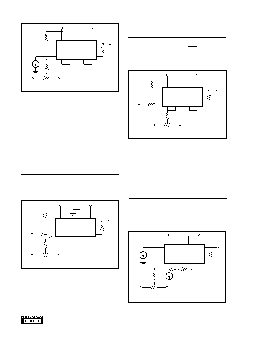
FIGURE 3. Transfer Function When I
1
is Negative.
ADJUSTMENT PROCEDURE
1. Refer to Choosing the Optimum Scale Factor and Refer-
ence Current.
2. Apply |I
1| = IR adjust R1 such that EO = 0.
3. Apply |I
1| = IMAX, adjust R2 for the proper output voltage
4. Repeat steps 2 and 3 if necessary.
5. Ignore this step if |I
1MIN| ≥ 10nA. Otherwise, apply |I1| =
1nA, make R
3 = 1kM and adjust R4 for the proper
output voltage. For R
3, a single resistor is recommended.
A voltage divider network is difficult to use due to
amplifier offset voltage.
Transfer function is E
O = –A log
, where E
1 is a
positive input voltage and I
R is the resistor-programmed
internal reference current (see Figure 4).
4. Apply E
1 = EMIN, adjust R3 for the proper output.
5. Repeat steps 2 through 4 if necessary.
Transfer function is E
O = –A log
, where E
1 is a
negative input voltage and I
R is the resistor-programmed
internal reference current (see Figure 5).
R
4
(1)
10k
R
3
(1)
–15VDC
+15VDC
7
23
22
14
21
4
2
51
4127
19
18
I
1
Reference
Current
+15VDC
–15VDC
Gain
R
2
E
O
NOTE: (1) Needed only
if I
1< 10nA.
E
1
R
4 IR
FIGURE 4. Transfer Function When E
1 is Positive.
R
3
10k
100M
–15VDC
+15VDC
4
23
22
14
21
4127
19
18
Reference
Current
+15VDC
–15VDC
Gain
R
2
E
O
E
1
10k
±1%
R
1
2
ADJUSTMENT PROCEDURE
1. Refer to Choosing the Optimum Scale Factor and
Reference Current.
2. Apply E
1 = IR (10k), adjust R1 such that EO = 0.
3. Apply E
1 = EMAX, adjust R2 for the proper output voltage.
ADJUSTMENT PROCEDURE
1. Refer to Choosing the Optimum Scale Factor and
Reference Current.
2. Apply |E
1| = IR (10k), adjust R1 such that EO = 0.
3. Apply |E
1| = EMAX, adjust R2 for the proper output voltage.
4. Apply |E
1| = EMIN, adjust R3 for the proper output.
5. Repeat steps 2 through 4 if necessary.
Transfer function is E
O
= –A log
with I
1 and
I
2
negative; |I
1| ≥ 1nA, |I2| ≥ 1A (see Figure 6).
FIGURE 5. Transfer Function When E
1 is Negative.
R
3
10k
100M
–15VDC
+15VDC
7
23
22
14
21
4
2
5
1
4127
19
18
Reference
Current
+15VDC
–15VDC
Gain
R
2
E
O
E
1
R
4
10k
±1%
R
1
|E
1|
R
4 IR
FIGURE 6. Transfer Function When I
1 and I2 are Negative.
R
4
(1)
10k
R
3
(1)
–15VDC
+15VDC
5
7
22
14
21
10
2
11
9
4127
19
18
I
1
+15VDC
–15VDC
Gain
E
O
I
2
4
R
5
(2)
R
6
(2)
NOTES:(1) Needed only
if |I
1| < 10nA.
(2) R
5 = R6 ±1%
|I
1|
|I
2|
相關PDF資料 |
PDF描述 |
|---|---|
| 41680 | Toroidal Surface Mount Inductors |
| 416R8 | Toroidal Surface Mount Inductors |
| 41100 | Toroidal Surface Mount Inductors |
| 41101 | Toroidal Surface Mount Inductors |
| 41150 | Toroidal Surface Mount Inductors |
相關代理商/技術參數 |
參數描述 |
|---|---|
| 412-7 | 功能描述:旋鈕開關 7 TAPS 50A/300VAC 20VDC RoHS:否 制造商:C&K Components 位置數量:5 卡片組數量: 每卡片組極數:2 電流額定值:250 mA 電壓額定值:125 V 指數角: 觸點類型: 觸點形式:DPST 端接類型:Solder 安裝類型:Panel 觸點電鍍:Silver |
| 41270.07 | 制造商:Vynckier Enclosure Systems Inc 功能描述:APO CARRY HANDLE |
| 412700000 | 功能描述:開關配件 STACKING SCREW 3XXX .950 RoHS:否 制造商:C&K Components 類型:Cap 用于:Pushbutton Switches 設計目的: |
| 4127010 | 制造商:Rittal 功能描述:DOOR SWITCH UL |
| 412701000 | 功能描述:開關配件 SCRW 3-4 FRNT 3 REAR RoHS:否 制造商:C&K Components 類型:Cap 用于:Pushbutton Switches 設計目的: |
發(fā)布緊急采購,3分鐘左右您將得到回復。