- 您現(xiàn)在的位置:買(mǎi)賣(mài)IC網(wǎng) > PDF目錄30629 > 4127 (Texas Instruments, Inc.) Logarithmic Amplifier(對(duì)數(shù)放大器) PDF資料下載
參數(shù)資料
| 型號(hào): | 4127 |
| 廠商: | Texas Instruments, Inc. |
| 元件分類(lèi): | 對(duì)數(shù)放大器 |
| 英文描述: | Logarithmic Amplifier(對(duì)數(shù)放大器) |
| 中文描述: | 對(duì)數(shù)放大器(對(duì)數(shù)放大器) |
| 文件頁(yè)數(shù): | 7/8頁(yè) |
| 文件大小: | 107K |
| 代理商: | 4127 |

4127
7
ADJUSTMENT PROCEDURE
1. Refer to Choosing the Optimum Scale Factor and
Reference Current.
2. No further adjustment is necessary if I
1 MIN ≥ 10nA,
otherwise connect the R
3 and R4 network, with R4 = 10k
and R
3 = 10
9
. Adjust R
4 for proper output voltage after
adjusting gain errors. Since the voltage at pin 4 is in the
range of
±5mV, it is not practical to use a T-network to
replace R
3.
Transfer function is E
O = –A log
with I
1 negative, I2
positive; |I
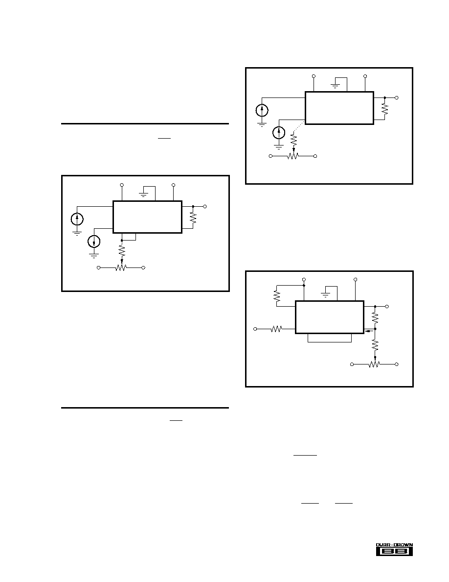
1| ≥ 1nA, I2 ≥ 1A (see Figure 7).
range of
±5mV, it is not practical to use a T-network to
replace R
3.
ANTILOG OPERATION
The 4127 can also perform the antilog function. The output
is connected through a resistor, R
O, into the current input, pin
4. The input signal is connected through a gain resistor to pin
19 as shown in Figure 9.
R
4
(1)
10k
R
3
(1)
I
2
–15VDC
+15VDC
7
2
22
14
21
4
5
4127
19
18
+15VDC
–15VDC
Gain
E
O
I
1
NOTE: (1) Needed only
if |I
1| < 10nA.
FIGURE 7. Transfer Function When I
1
is Negative, I
2
is
Positive.
FIGURE 9. Antilog Operation.
10k
Offset Adjust
≈100M
–15VDC
+15VDC
19
23
22
14
21
4127
4
18
Ref.
+15VDC
–15VDC
R
O
E
O
E
S
R
2
R
1
2
I
S
Insert 0.01F between
Pin 18 and Pin 19 if the
unit oscillates.
These connections form an implicit loop for computing the
antilog function. From the block diagram of Figure 1, the
voltage at the inverting input of the output amplifier A
2 must
equal E
2, so
E
2 ≈
E
S, RT ≈ 520
Since the output is connected through R
O to pin 4, the current
I
S will equal EO/RO and E2 will be
E
2 = –
n
E
O
mKT
q
l
R
T + R2
R
T
R
OIR
ADJUSTMENT PROCEDURE
1. Refer to Choosing the Optimum Scale Factor and
Reference Current.
2. No further adjustment is necessary if |I
1|MIN ≥
10nA,
otherwise connect the R
3 and R4 network, with R4 = 10k
and R
3 = 10
9
. Adjust R
4 for proper output voltage after
adjusting gain errors. Since the voltage at pin 4 is in the
range of
±5mV, it is not practical to use a T-network to
replace R
3.
.
Transfer function is E
O
= –A log
with I
1
and I
2
positive; I
1 ≥ 1nA, I2 ≥ 1A (see Figure 8).
ADJUSTMENT PROCEDURE
1. Refer to Choosing the Optimum Scale Factor and
Reference Current.
2. No further adjustment is necessary if I
1 MIN ≥ 10nA,
otherwise connect the R
3 and R4 network, with R4 = 10k
and R
3 = 10
9
. Adjust R
4 for proper output voltage after
adjusting gain errors. Since the voltage at pin 4 is in the
I
1
I
2
|I
1|
I
2
FIGURE 8. Transfer Function When I
1 and I2 is Positive.
R
4
(1)
10k
R
3
(1)
I
2
–15VDC
+15VDC
4
2
22
14
21
4127
19
18
+15VDC
–15VDC
Gain
E
O
I
1
NOTE: (1) Needed only
if |I
1| < 10nA.
相關(guān)PDF資料 |
PDF描述 |
|---|---|
| 41680 | Toroidal Surface Mount Inductors |
| 416R8 | Toroidal Surface Mount Inductors |
| 41100 | Toroidal Surface Mount Inductors |
| 41101 | Toroidal Surface Mount Inductors |
| 41150 | Toroidal Surface Mount Inductors |
相關(guān)代理商/技術(shù)參數(shù) |
參數(shù)描述 |
|---|---|
| 412-7 | 功能描述:旋鈕開(kāi)關(guān) 7 TAPS 50A/300VAC 20VDC RoHS:否 制造商:C&K Components 位置數(shù)量:5 卡片組數(shù)量: 每卡片組極數(shù):2 電流額定值:250 mA 電壓額定值:125 V 指數(shù)角: 觸點(diǎn)類(lèi)型: 觸點(diǎn)形式:DPST 端接類(lèi)型:Solder 安裝類(lèi)型:Panel 觸點(diǎn)電鍍:Silver |
| 41270.07 | 制造商:Vynckier Enclosure Systems Inc 功能描述:APO CARRY HANDLE |
| 412700000 | 功能描述:開(kāi)關(guān)配件 STACKING SCREW 3XXX .950 RoHS:否 制造商:C&K Components 類(lèi)型:Cap 用于:Pushbutton Switches 設(shè)計(jì)目的: |
| 4127010 | 制造商:Rittal 功能描述:DOOR SWITCH UL |
| 412701000 | 功能描述:開(kāi)關(guān)配件 SCRW 3-4 FRNT 3 REAR RoHS:否 制造商:C&K Components 類(lèi)型:Cap 用于:Pushbutton Switches 設(shè)計(jì)目的: |
發(fā)布緊急采購(gòu),3分鐘左右您將得到回復(fù)。