- 您現(xiàn)在的位置:買賣IC網 > PDF目錄67328 > 5962-8967601XX (CIRRUS LOGIC INC) 1-CH 16-BIT SUCCESSIVE APPROXIMATION ADC, SERIAL/PARALLEL ACCESS, CQCC44 PDF資料下載
參數資料
| 型號: | 5962-8967601XX |
| 廠商: | CIRRUS LOGIC INC |
| 元件分類: | ADC |
| 英文描述: | 1-CH 16-BIT SUCCESSIVE APPROXIMATION ADC, SERIAL/PARALLEL ACCESS, CQCC44 |
| 封裝: | CERAMIC, LCC-44 |
| 文件頁數: | 5/50頁 |
| 文件大小: | 520K |
| 代理商: | 5962-8967601XX |
第1頁第2頁第3頁第4頁當前第5頁第6頁第7頁第8頁第9頁第10頁第11頁第12頁第13頁第14頁第15頁第16頁第17頁第18頁第19頁第20頁第21頁第22頁第23頁第24頁第25頁第26頁第27頁第28頁第29頁第30頁第31頁第32頁第33頁第34頁第35頁第36頁第37頁第38頁第39頁第40頁第41頁第42頁第43頁第44頁第45頁第46頁第47頁第48頁第49頁第50頁

All calibration, conversion, and throughput times
directly scale to CLKIN frequency. Thus,
throughput can be precisely controlled and/or
maximized using an external CLKIN signal. In
contrast, the CS5012A/14/16’s internal oscillator
will vary from unit-to-unit and over temperature.
The CS5012A/14/16 can typically convert with
CLKIN as low as 10 kHz at room temperature.
Initiating Conversions
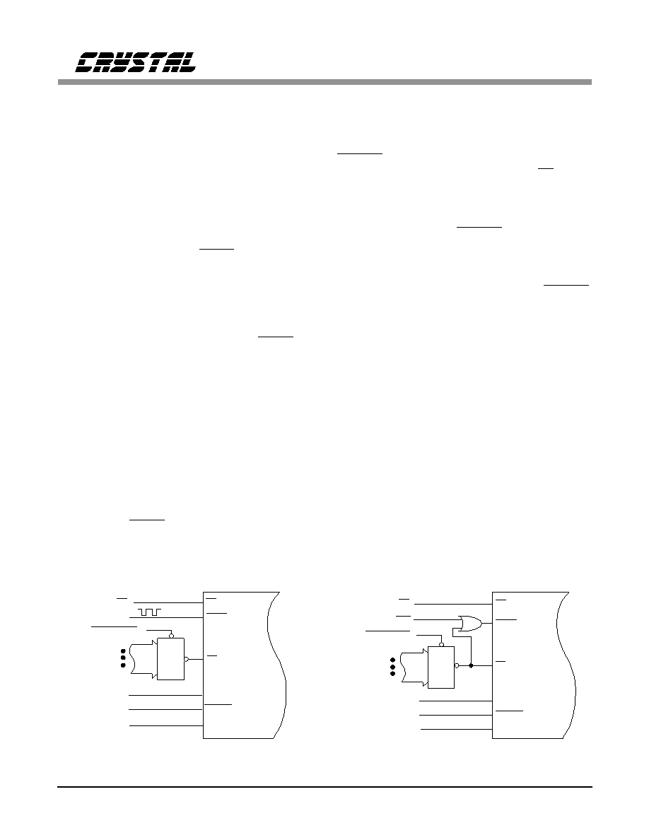
A falling transition on the HOLD pin places the
input in the hold mode and initiates a conversion
cycle. Upon completion of the conversion cycle,
the CS5012A/14/16 automatically return to the
track mode. In contrast to systems with separate
track-and-holds and A/D converters, a sampling
clock can simply be connected to the HOLD in-
put (Figure 3a). The duty cycle of this clock is
not critical. It need only remain low at least one
CLKIN cycle plus 50 ns, but no longer than the
minimum conversion time or an additional con-
version cycle will be initiated with inadequate
time for acquisition.
Microprocessor-Controlled Operation
Sampling and conversion can be placed under
microprocessor control (Figure 4) by simply gat-
ing the devices’ decoded address with the write
strobe for the HOLD input. Thus, a write cycle to
the CS5012A/14/16’s base address will initiate a
conversion. However, the write cycle must be to
the odd address (A0 high) to avoid initiating a
software controlled reset (see Reset below).
The calibration control inputs, CAL, and
INTRLV are inputs to a set of transparent latches.
These signals are internally latched by CS return-
ing high. They must be in the appropriate state
whenever the chip is selected during a read or
write cycle. Address lines A1 and A2 are shown
connected to CAL and INTRLV in Figure 4 plac-
ing calibration under microprocessor control as
well. Thus, any read or write cycle to the
CS5012A/14/16’s base address will initiate or ter-
minate calibration. Alternatively, A0, INTRLV,
and CAL may be connected to the microproces-
sor data bus.
Conversion Time/Throughput
Upon completing a conversion cycle and return-
ing to the track mode, the CS5012A/14/16
require time to acquire the analog input signal
before another conversion can be initiated. The
acquisition time is specified as six CLKIN cycles
plus 2.25
s (1.32 s for the CS5012A -7 version
only). This adds to the conversion time to define
the converter’s maximum throughput. The con-
version time of the CS5012A/14/16, in turn,
depends on the sampling, calibration, and CLKIN
conditions.
HOLD
CS5012A/14/16
Addr
Dec
A3
AN
Address
Bus
WR
RD
CS
RD
INTRLV
A2
A1
CAL
A0
ADDR VALID
Figure 4b. Conversions under Microprocessor Control
CS5012A/14/16
CS
Addr
Dec
A3
AN
Address
Bus
RD
CONCLK
HOLD
INTRLV
CAL
A0
A2
A1
A0
ADDR VALID
Figure 4a. Conversions Asynchronous to CLKIN
CS5012A, CS5014, CS5016
DS14F6
13
相關PDF資料 |
PDF描述 |
|---|---|
| 5962-8967602QX | 1-CH 16-BIT SUCCESSIVE APPROXIMATION ADC, SERIAL/PARALLEL ACCESS, CDIP40 |
| 5962-8967602XX | 1-CH 16-BIT SUCCESSIVE APPROXIMATION ADC, SERIAL/PARALLEL ACCESS, CQCC44 |
| 5962-8967402QX | 1-CH 14-BIT SUCCESSIVE APPROXIMATION ADC, SERIAL/PARALLEL ACCESS, CDIP40 |
| 5962-8967901XX | 1-CH 12-BIT SUCCESSIVE APPROXIMATION ADC, SERIAL/PARALLEL ACCESS, CQCC44 |
| 5962-8967402XX | 1-CH 14-BIT SUCCESSIVE APPROXIMATION ADC, SERIAL/PARALLEL ACCESS, CQCC44 |
相關代理商/技術參數 |
參數描述 |
|---|---|
| 5962-8967701CA | 制造商:Linear Technology 功能描述:AMPLIFIER-OP AMP 制造商:Texas Instruments 功能描述:OP Amp Quad GP ±22V/44V 14-Pin CDIP Tube 制造商:Texas Instruments 功能描述:OP AMP QUAD GP 22V/44V 14CDIP - Rail/Tube 制造商:Texas Instruments 功能描述:LT1014AMJB QUAD PREC OP AMP |
| 5962-8967702CA | 制造商:Texas Instruments 功能描述:OP Amp Quad GP ±22V/44V 14-Pin CDIP Tube 制造商:Texas Instruments 功能描述:OP AMP QUAD GP 22V/44V 14CDIP - Rail/Tube |
| 5962-8967801XA | 制造商:Rochester Electronics LLC 功能描述:- Bulk 制造商:Analog Devices 功能描述: |
| 5962-8967802XA | 制造商:Rochester Electronics LLC 功能描述:8-BIT QUAD MULT DAC IC - Bulk 制造商:Analog Devices 功能描述: |
| 5962-8967901XC | 制造商:SEI 功能描述: |
發(fā)布緊急采購,3分鐘左右您將得到回復。