- 您現(xiàn)在的位置:買賣IC網(wǎng) > PDF目錄68796 > 5962-90604042A (TEXAS INSTRUMENTS INC) QUAD OP-AMP, 3750 uV OFFSET-MAX, 0.525 MHz BAND WIDTH, CQCC20 PDF資料下載
參數(shù)資料
| 型號: | 5962-90604042A |
| 廠商: | TEXAS INSTRUMENTS INC |
| 元件分類: | 運算放大器 |
| 英文描述: | QUAD OP-AMP, 3750 uV OFFSET-MAX, 0.525 MHz BAND WIDTH, CQCC20 |
| 封裝: | CERAMIC, LCC-20 |
| 文件頁數(shù): | 12/43頁 |
| 文件大小: | 762K |
| 代理商: | 5962-90604042A |
第1頁第2頁第3頁第4頁第5頁第6頁第7頁第8頁第9頁第10頁第11頁當前第12頁第13頁第14頁第15頁第16頁第17頁第18頁第19頁第20頁第21頁第22頁第23頁第24頁第25頁第26頁第27頁第28頁第29頁第30頁第31頁第32頁第33頁第34頁第35頁第36頁第37頁第38頁第39頁第40頁第41頁第42頁第43頁

TLC27M4, TLC27M4A, TLC27M4B, TLC27M4Y, TLC27M9
LinCMOS
PRECISION QUAD OPERATIONAL AMPLIFIERS
SLOS093C – OCTOBER 1987 – REVISED MAY 1999
2
POST OFFICE BOX 655303
DALLAS, TEXAS 75265
description (continued)
Four offset voltage grades are available (C-suffix and I-suffix types), ranging from the low-cost TLC27M4 (10
mV) to the high-precision TLC27M9 (900
V). These advantages, in combination with good common-mode
rejection and supply voltage rejection, make these devices a good choice for new state-of-the-art designs as
well as for upgrading existing designs.
In general, many features associated with bipolar technology are available on LinCMOS
operational
amplifiers, without the power penalties of bipolar technology. General applications such as transducer
interfacing, analog calculations, amplifier blocks, active filters, and signal buffering are easily designed with the
TLC27M4 and TLC27M9. The devices also exhibit low voltage single-supply operation, and low power
consumption, making them ideally suited for remote and inaccessible battery-powered applications. The
common-mode input voltage range includes the negative rail.
A wide range of packaging options is available, including small-outline and chip-carrier versions for high-density
system applications.
The device inputs and outputs are designed to withstand – 100-mA surge currents without sustaining latch-up.
The TLC27M4 and TLC27M9 incorporate internal ESD-protection circuits that prevent functional failures at
voltages up to 2000 V as tested under MIL-STD-883C, Method 3015; however, care should be exercised in
handling these devices, as exposure to ESD may result in the degradation of the device parametric
performance.
The C-suffix devices are characterized for operation from 0
°C to 70°C. The I-suffix devices are characterized
for operation from – 40
°C to 85°C. The M-suffix devices are characterized for operation over the full military
temperature range of – 55
°C to 125°C.
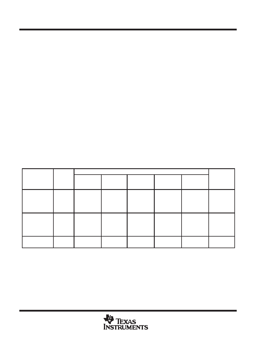
AVAILABLE OPTIONS
PACKAGE
CHIP
TA
VIOmax
AT 25
°C
SMALL
OUTLINE
(D)
CHIP
CARRIER
(FK)
CERAMIC
DIP
(J)
PLASTIC
DIP
(N)
TSSOP
(PW)
CHIP
FORM
(Y)
900
V
TLC27M9CD
—
TLC27M9CN
—
0
°Cto70°C
2 mV
TLC27M4BCD
—
TLC27M4BCN
—
0
°C to 70°C
5 mV
TLC27M4ACD
—
TLC27M4ACN
—
10 mV
TLC27M4CD
—
TLC27M4CN
TLC27M4CPW
TLC27M4Y
900
V
TLC27M9ID
—
TLC27M9IN
—
40
°Cto85°C
2 mV
TLC27M4BID
—
TLC27M4BIN
—
– 40
°C to 85°C
5 mV
TLC27M4AID
—
TLC27M4AIN
—
10 mV
TLC27M4ID
—
TLC27M4IN
TLC27M41PW
—
55
°Cto125°C
900
V
TLC27M9MD
TLC27M9MFK
TLC27M9MJ
TLC27M9MN
—
– 55
°C to 125°C
10 mV
TLC27M4MD
TLC27M4MFK
TLC27M4MJ
TLC27M4MN
—
The D and PW package is available taped and reeled. Add R suffix to the device type (e.g., TLC279CDR).
相關(guān)PDF資料 |
PDF描述 |
|---|---|
| 5962-9081201MGA | BUFFER AMPLIFIER, MBCY8 |
| 5962-9081201MPA | BUFFER AMPLIFIER, CDIP8 |
| 5962-9088102M2A | DUAL OP-AMP, 700 uV OFFSET-MAX, 2.8 MHz BAND WIDTH, CQCC20 |
| 5962-9088102MPA | DUAL OP-AMP, 700 uV OFFSET-MAX, 2.8 MHz BAND WIDTH, CDIP8 |
| 5962-9088105Q2A | DUAL OP-AMP, 450 uV OFFSET-MAX, 2.8 MHz BAND WIDTH, CQCC20 |
相關(guān)代理商/技術(shù)參數(shù) |
參數(shù)描述 |
|---|---|
| 5962-9060404CA | 制造商:Rochester Electronics LLC 功能描述:- Bulk |
| 5962-90604052A | 制造商:Rochester Electronics LLC 功能描述:- Bulk |
| 5962-90606022A | 制造商:e2v Aerospace & Defense 功能描述:SMD MKD 54F112 LCC FSC |
| 5962-9060602EA | 制造商:e2v Aerospace & Defense 功能描述:SMD MKD 54F112 FSC-DIP |
| 5962-9060602FA | 制造商:e2v Aerospace & Defense 功能描述:SMD MKD 54F112 FP-FSC |
發(fā)布緊急采購,3分鐘左右您將得到回復(fù)。