- 您現(xiàn)在的位置:買(mǎi)賣(mài)IC網(wǎng) > PDF目錄68796 > 5962-90604042A (TEXAS INSTRUMENTS INC) QUAD OP-AMP, 3750 uV OFFSET-MAX, 0.525 MHz BAND WIDTH, CQCC20 PDF資料下載
參數(shù)資料
| 型號(hào): | 5962-90604042A |
| 廠商: | TEXAS INSTRUMENTS INC |
| 元件分類: | 運(yùn)算放大器 |
| 英文描述: | QUAD OP-AMP, 3750 uV OFFSET-MAX, 0.525 MHz BAND WIDTH, CQCC20 |
| 封裝: | CERAMIC, LCC-20 |
| 文件頁(yè)數(shù): | 27/43頁(yè) |
| 文件大?。?/td> | 762K |
| 代理商: | 5962-90604042A |
第1頁(yè)第2頁(yè)第3頁(yè)第4頁(yè)第5頁(yè)第6頁(yè)第7頁(yè)第8頁(yè)第9頁(yè)第10頁(yè)第11頁(yè)第12頁(yè)第13頁(yè)第14頁(yè)第15頁(yè)第16頁(yè)第17頁(yè)第18頁(yè)第19頁(yè)第20頁(yè)第21頁(yè)第22頁(yè)第23頁(yè)第24頁(yè)第25頁(yè)第26頁(yè)當(dāng)前第27頁(yè)第28頁(yè)第29頁(yè)第30頁(yè)第31頁(yè)第32頁(yè)第33頁(yè)第34頁(yè)第35頁(yè)第36頁(yè)第37頁(yè)第38頁(yè)第39頁(yè)第40頁(yè)第41頁(yè)第42頁(yè)第43頁(yè)

TLC27M4, TLC27M4A, TLC27M4B, TLC27M4Y, TLC27M9
LinCMOS
PRECISION QUAD OPERATIONAL AMPLIFIERS
SLOS093C – OCTOBER 1987 – REVISED MAY 1999
33
POST OFFICE BOX 655303
DALLAS, TEXAS 75265
APPLICATION INFORMATION
output characteristics (continued)
Although the TLC27M4 and TLC27M9 possess excellent high-level output voltage and current capability,
methods for boosting this capability are available, if needed. The simplest method involves the use of a pullup
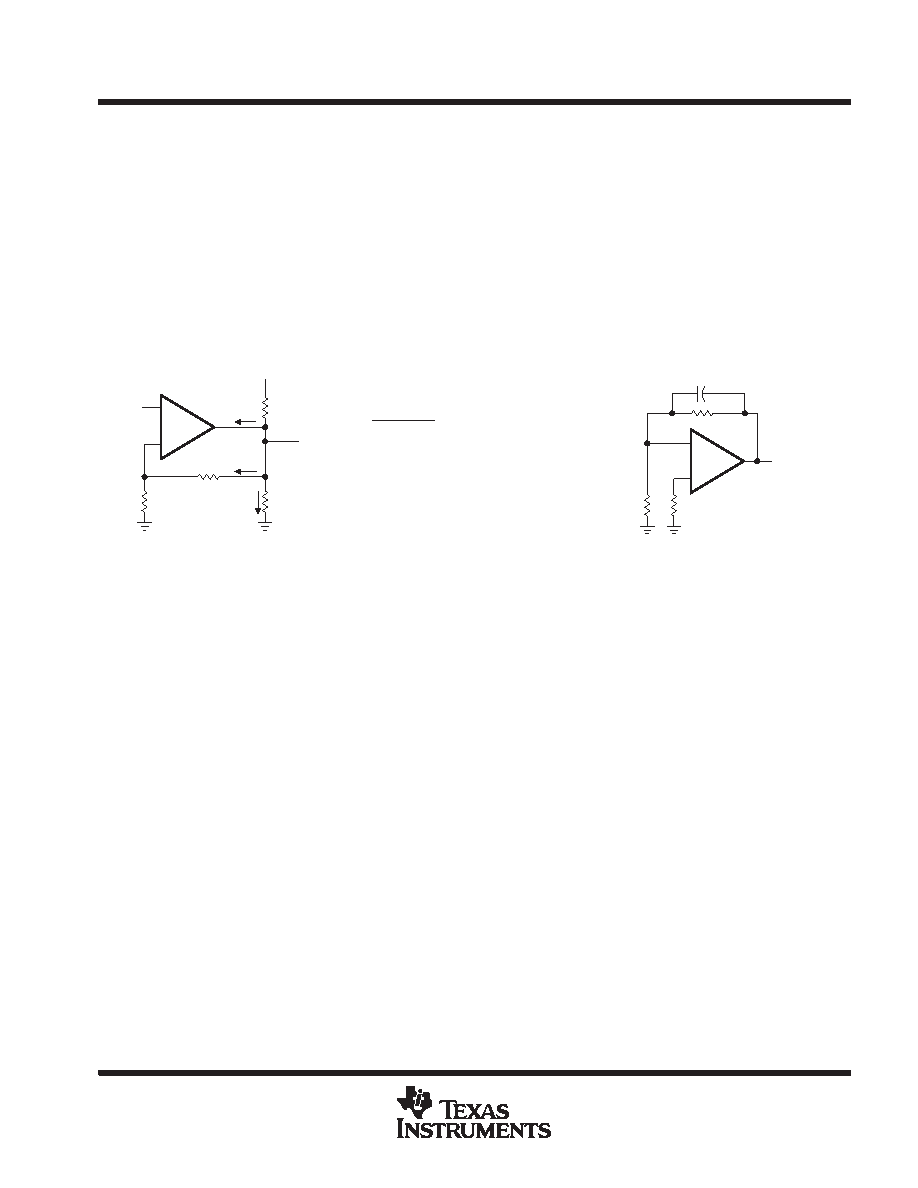
resistor (RP) connected from the output to the positive supply rail (see Figure 42). There are two disadvantages
to the use of this circuit. First, the NMOS pulldown transistor N4 (see equivalent schematic) must sink a
comparatively large amount of current. In this circuit, N4 behaves like a linear resistor with an on-resistance
between approximately 60
and 180 , depending on how hard the operational amplifier input is driven. With
very low values of RP, a voltage offset from 0 V at the output occurs. Second, pullup resistor RP acts as a drain
load to N4 and the gain of the operational amplifier is reduced at output voltage levels where N5 is not supplying
the output current.
–
+
VI
VDD
RP
VO
R2
R1
RL
IP
IF
IL
–
+
C
IP = Pullup current required
by the operational amplifier
(typically 500
A)
VO
Rp =
VDD – VO
IF + IL + IP
Figure 42. Resistive Pullup
Figure 43. Compensation for
to Increase VOH
Input Capacitance
feedback
Operational amplifier circuits nearly always employ feedback, and since feedback is the first prerequisite for
oscillation, some caution is appropriate. Most oscillation problems result from driving capacitive loads
(discussed previously) and ignoring stray input capacitance. A small-value capacitor connected in parallel with
the feedback resistor is an effective remedy (see Figure 43). The value of this capacitor is optimized empirically.
electrostatic discharge protection
The TLC27M4 and TLC27M9 incorporate an internal electrostatic discharge (ESD) protection circuit that
prevents functional failures at voltages up to 2000 V as tested under MIL-STD-883C, Method 3015.2. Care
should be exercised, however, when handling these devices, as exposure to ESD may result in the degradation
of the device parametric performance. The protection circuit also causes the input bias currents to be
temperature-dependent and have the characteristics of a reverse-biased diode.
latch-up
Because CMOS devices are susceptible to latch-up due to their inherent parasitic thyristors, the TLC27M4 and
TLC27M9 inputs and outputs were designed to withstand – 100-mA surge currents without sustaining latch-up;
however, techniques should be used to reduce the chance of latch-up whenever possible. Internal protection
diodes should not, by design, be forward biased. Applied input and output voltage should not exceed the supply
voltage by more than 300 mV. Care should be exercised when using capacitive coupling on pulse generators.
Supply transients should be shunted by the use of decoupling capacitors (0.1
F typical) located across the
supply rails as close to the device as possible.
相關(guān)PDF資料 |
PDF描述 |
|---|---|
| 5962-9081201MGA | BUFFER AMPLIFIER, MBCY8 |
| 5962-9081201MPA | BUFFER AMPLIFIER, CDIP8 |
| 5962-9088102M2A | DUAL OP-AMP, 700 uV OFFSET-MAX, 2.8 MHz BAND WIDTH, CQCC20 |
| 5962-9088102MPA | DUAL OP-AMP, 700 uV OFFSET-MAX, 2.8 MHz BAND WIDTH, CDIP8 |
| 5962-9088105Q2A | DUAL OP-AMP, 450 uV OFFSET-MAX, 2.8 MHz BAND WIDTH, CQCC20 |
相關(guān)代理商/技術(shù)參數(shù) |
參數(shù)描述 |
|---|---|
| 5962-9060404CA | 制造商:Rochester Electronics LLC 功能描述:- Bulk |
| 5962-90604052A | 制造商:Rochester Electronics LLC 功能描述:- Bulk |
| 5962-90606022A | 制造商:e2v Aerospace & Defense 功能描述:SMD MKD 54F112 LCC FSC |
| 5962-9060602EA | 制造商:e2v Aerospace & Defense 功能描述:SMD MKD 54F112 FSC-DIP |
| 5962-9060602FA | 制造商:e2v Aerospace & Defense 功能描述:SMD MKD 54F112 FP-FSC |
發(fā)布緊急采購(gòu),3分鐘左右您將得到回復(fù)。