- 您現(xiàn)在的位置:買賣IC網(wǎng) > PDF目錄68796 > 5962-9089504QCA (TEXAS INSTRUMENTS INC) OP-AMP, 40 uV OFFSET-MAX, 1.9 MHz BAND WIDTH, CDIP14 PDF資料下載
參數(shù)資料
| 型號(hào): | 5962-9089504QCA |
| 廠商: | TEXAS INSTRUMENTS INC |
| 元件分類: | 運(yùn)算放大器 |
| 英文描述: | OP-AMP, 40 uV OFFSET-MAX, 1.9 MHz BAND WIDTH, CDIP14 |
| 封裝: | CERAMIC, DIP-14 |
| 文件頁(yè)數(shù): | 15/36頁(yè) |
| 文件大?。?/td> | 916K |
| 代理商: | 5962-9089504QCA |
第1頁(yè)第2頁(yè)第3頁(yè)第4頁(yè)第5頁(yè)第6頁(yè)第7頁(yè)第8頁(yè)第9頁(yè)第10頁(yè)第11頁(yè)第12頁(yè)第13頁(yè)第14頁(yè)當(dāng)前第15頁(yè)第16頁(yè)第17頁(yè)第18頁(yè)第19頁(yè)第20頁(yè)第21頁(yè)第22頁(yè)第23頁(yè)第24頁(yè)第25頁(yè)第26頁(yè)第27頁(yè)第28頁(yè)第29頁(yè)第30頁(yè)第31頁(yè)第32頁(yè)第33頁(yè)第34頁(yè)第35頁(yè)第36頁(yè)

TLC2654, TLC2654A
Advanced LinCMOS
LOW-NOISE CHOPPER-STABILIZED
OPERATIONAL AMPLIFIERS
SLOS020G – NOVEMBER 1988 – REVISED APRIL 2001
22
POST OFFICE BOX 655303
DALLAS, TEXAS 75265
APPLICATION INFORMATION
theory of operation (continued)
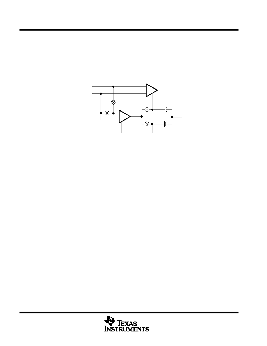
During the nulling phase, switch A is closed, shorting the nulling amplifier inputs together and allowing the nulling
amplifier to reduce its own input offset voltage by feeding its output signal back to an inverting input node.
Simultaneously, external capacitor CXA stores the nulling potential to allow the offset voltage of the amplifier to
remain nulled during the amplifying phase.
Null
IN +
IN –
Main
VDD –
CXA
CXB
B
A
B
A
+
–
5
4
10
OUT
7
Pin numbers shown are for the D (14 pin), J, and N packages.
Figure 35. TLC2654 Simplified Block Diagram
During the amplifying phase, switch B is closed, connecting the output of the nulling amplifier to a noninverting
input of the main amplifier. In this configuration, the input offset voltage of the main amplifier is nulled. Also,
external capacitor CXB stores the nulling potential to allow the offset voltage of the main amplifier to remain
nulled during the next nulling phase.
This continuous chopping process allows offset voltage nulling during variations in time and temperature and
over the common-mode input voltage range and power supply range. In addition, because the low-frequency
signal path is through both the null and main amplifiers, extremely high gain is achieved.
The low-frequency noise of a chopper amplifier depends on the magnitude of the component noise prior to
chopping and the capability of the circuit to reduce this noise while chopping. The use of the Advanced LinCMOS
process, with its low-noise analog MOS transistors and patent-pending input stage design, significantly reduces
the input noise voltage.
The primary source of nonideal operation in chopper-stabilized amplifiers is error charge from the switches. As
charge imbalance accumulates on critical nodes, input offset voltage can increase especially with increasing
chopping frequency. This problem has been significantly reduced in the TLC2654 by use of a patent-pending
compensation circuit and the Advanced LinCMOS process.
The TLC2654 incorporates a feed-forward design that ensures continuous frequency response. Essentially, the
gain magnitude of the nulling amplifier and compensation network crosses unity at the break frequency of the
main amplifier. As a result, the high-frequency response of the system is the same as the frequency response
of the main amplifier. This approach also ensures that the slewing characteristics remain the same during both
the nulling and amplifying phases.
The primary limitation on ac performance is the chopping frequency. As the input signal frequency approaches
the chopper’s clock frequency, intermodulation (or aliasing) errors result from the mixing of these frequencies.
To avoid these error signals, the input frequency must be less than half the clock frequency. Most choppers
available today limit the internal chopping frequency to less than 500 Hz in order to eliminate errors due to the
charge imbalancing phenomenon mentioned previously. However, to avoid intermodulation errors on a 500-Hz
chopper, the input signal frequency must be limited to less than 250 Hz.
相關(guān)PDF資料 |
PDF描述 |
|---|---|
| 5962-9089504QPA | OP-AMP, 40 uV OFFSET-MAX, 1.9 MHz BAND WIDTH, CDIP8 |
| 5962-9089502M2A | OP-AMP, 50 uV OFFSET-MAX, 1.9 MHz BAND WIDTH, CQCC20 |
| 5962-9089601M2A | OP-AMP, 105 uV OFFSET-MAX, 13 MHz BAND WIDTH, CQCC20 |
| 5962-9089601MPA | OP-AMP, 105 uV OFFSET-MAX, 13 MHz BAND WIDTH, CDIP8 |
| 5962-9089603Q2A | OP-AMP, 105 uV OFFSET-MAX, 13 MHz BAND WIDTH, CQCC20 |
相關(guān)代理商/技術(shù)參數(shù) |
參數(shù)描述 |
|---|---|
| 5962-9089504QPA | 制造商:Texas Instruments 功能描述:SP Amp Chopper Stabilization Single |
| 5962-9089601M2A | 制造商:Texas Instruments 功能描述:OP Amp Single GP 制造商:Texas Instruments 功能描述:OP AMP SGL GP 19V 20LCCC - Rail/Tube |
| 5962-9089601MPA | 制造商:Texas Instruments 功能描述:OP Amp Single GP |
| 5962-9089603Q2A | 制造商:Texas Instruments 功能描述:OP Amp Single GP 制造商:Texas Instruments 功能描述:OP AMP SGL GP 19V 20LCCC - Rail/Tube |
| 5962-9089901M | 制造商:Rochester Electronics LLC 功能描述:- Bulk |
發(fā)布緊急采購(gòu),3分鐘左右您將得到回復(fù)。