- 您現(xiàn)在的位置:買(mǎi)賣(mài)IC網(wǎng) > PDF目錄56735 > 5962-9161301HZX 2-OUTPUT 30 W DC-DC REG PWR SUPPLY MODULE PDF資料下載
參數(shù)資料
| 型號(hào): | 5962-9161301HZX |
| 元件分類: | 電源模塊 |
| 英文描述: | 2-OUTPUT 30 W DC-DC REG PWR SUPPLY MODULE |
| 封裝: | FM-10 |
| 文件頁(yè)數(shù): | 3/9頁(yè) |
| 文件大小: | 113K |
| 代理商: | 5962-9161301HZX |
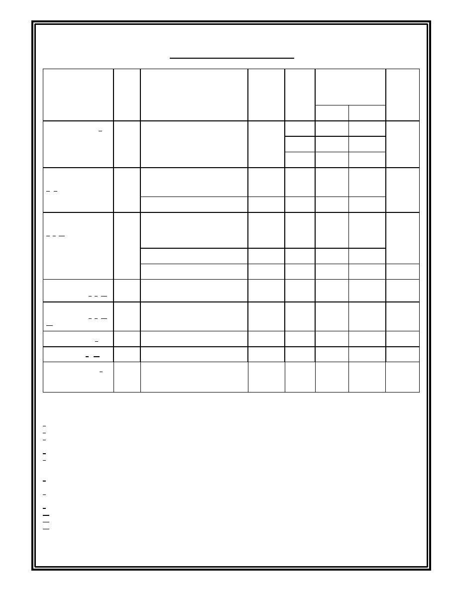
3
ATW2812D
TABLE I. Electrical Performance Characteristics - Continued
Test
Symbol
Conditions
-55
°C ≤ T
C
≤ +125°C
VIN = 28 V dc ±5%, CL = 0 unless
otherwise specified
Group A
Subgroups
Device
types
Limits
Unit
Min
Max
Switching frequency 4/
FS
IOUT = 2500 mA
4,5,6
01
250
300
KHz
02
250
270
03
275
300
Output response to step
transient load changes
4/ 9/
VOTLOA
D
1250 mA to/from 2500 mA
4,5,6
All
-400
+400
mV pk
0 mA to/from 2500 mA
4,5,6
All
-800
+800
Recovery time, step
transient load changes
4/ 9/ 10/
TTLOAD
1250 mA to/from 2500 mA
4,5,6
All
70
s
0 mA to/from 1250 mA
4,5,6
All
500
1250 mA to/from 0 mA
4,5,6
All
5
ms
Output response transient
step line changes 4/ 7/ 11/
VOTLINE
Input step from/to 18 to 40 V dc,
IOUT = 2500 mA
4,5,6
All
-800
+800
mV pk
Recovery time transient
step line changes 4/ 7/ 10/
11/
TTLINE
Input step from/to 18 to
40 V dc,
IOUT = 2500 mA
4,5,6
All
4000
s
Turn on overshoot 4/
VTonOS
IOUT = 0 and 2500 mA
4,5,6
All
750
mV pk
Turn on delay
4/ 12/
TonD
IOUT = 0 and 2500 mA
4,5,6
All
14
ms
Load fault recovery
7/
TrLF
4,5,6
All
14
ms
Weight
Flange
75
grams
Notes:
1/
Parameter guaranteed by line load, and cross regulation tests.
2/
Up to 90 percent of full power is available from either output provided the total output does not exceed 30 W.
3/
Bandwidth guaranteed by design. Tested for 20 KHz to 2 MHz.
4/
Load current split equally between +VOUT and -VOUT.
5/
Three-watt load on output under test, 3 watt to 27 watt load change on other output.
6/
Capacitive load may be any value from 0 to the maximum limit without compromising dc performance. A capacitive load in excess of the
maximum limit will not disturb loop stability but may interfere with the operation of the load fault detection circuitry, appearing as a short circuit during
turn-on.
7/
Parameter shall be tested as part of design characterization and after design or process changes. Thereafter, parameters shall be guaranteed to the limits
specified in Table I.
8/
An overload is that condition with a load in excess of the rated load but less than that necessary to trigger the short circuit protection and is the condition
of maximum power dissipation.
9/
Load step transition time between 2 and 10 microseconds.
10/
Recovery time is measured from the initiation of the transient to where VOUT has returned to within ±1 percent of VOUT at 50 percent load.
11/
Input step transition time between 2 and 10 microseconds.
12/
Turn-on delay time measurement is for either a step application of power at the input or the removal of a ground signal from the inhibit pin (pin 8) while
power is applied to the input.
相關(guān)PDF資料 |
PDF描述 |
|---|---|
| 5962-9210901HZX | 2-OUTPUT 30 W DC-DC REG PWR SUPPLY MODULE |
| 5962-9210902HZX | 2-OUTPUT 30 W DC-DC REG PWR SUPPLY MODULE |
| 5962-9161302HZX | 2-OUTPUT 30 W DC-DC REG PWR SUPPLY MODULE |
| 5962-9161303HZX | 2-OUTPUT 30 W DC-DC REG PWR SUPPLY MODULE |
| 5962-9161302HZA | 2-OUTPUT 30 W DC-DC REG PWR SUPPLY MODULE |
相關(guān)代理商/技術(shù)參數(shù) |
參數(shù)描述 |
|---|---|
| 5962-9161302HZA | 制造商:International Rectifier 功能描述:DC/DC CONVERTER, FLANGED, CLASS H, SLAVE - Rail/Tube |
| 5962-9161303HZA | 制造商:International Rectifier 功能描述:DC/DC CONVERTER, FLANGED, CLASS H, MASTER - Rail/Tube |
| 5962-9161701MXA | 功能描述:靜態(tài)隨機(jī)存取存儲(chǔ)器 RoHS:否 制造商:Cypress Semiconductor 存儲(chǔ)容量:16 Mbit 組織:1 M x 16 訪問(wèn)時(shí)間:55 ns 電源電壓-最大:3.6 V 電源電壓-最小:2.2 V 最大工作電流:22 uA 最大工作溫度:+ 85 C 最小工作溫度:- 40 C 安裝風(fēng)格:SMD/SMT 封裝 / 箱體:TSOP-48 封裝:Tray |
| 5962-9161702MXA | 制造商:Integrated Device Technology Inc 功能描述:SRAM ASYNC DUAL 5V 128KBIT 8KX16 70NS 84PIN PGA - Rail/Tube |
| 5962-9161702MYA | 制造商:Integrated Device Technology Inc 功能描述:SRAM ASYNC DUAL 5V 128KBIT 8KX16 70NS 84PIN FPAK - Rail/Tube |
發(fā)布緊急采購(gòu),3分鐘左右您將得到回復(fù)。