- 您現(xiàn)在的位置:買賣IC網(wǎng) > PDF目錄157277 > 5962-9561328H9C (AUSTIN SEMICONDUCTOR INC) 512K X 8 STANDARD SRAM, 12 ns, CDFP32 PDF資料下載
參數(shù)資料
| 型號: | 5962-9561328H9C |
| 廠商: | AUSTIN SEMICONDUCTOR INC |
| 元件分類: | SRAM |
| 英文描述: | 512K X 8 STANDARD SRAM, 12 ns, CDFP32 |
| 封裝: | CERAMIC, DFP-32 |
| 文件頁數(shù): | 13/17頁 |
| 文件大小: | 112K |
| 代理商: | 5962-9561328H9C |
SRAM
AS5C4008
AS5C4008
Rev. 6.2 06/05
Austin Semiconductor, Inc. reserves the right to change products or specifications without notice.
5
Austin Semiconductor, Inc.
NOTES
1.
All voltages referenced to V
SS (GND).
2.
-2V for pulse width < 20ns
3.
I
CC is dependent on output loading and cycle rates.
4.
This parameter is guaranteed but not tested.
5.
Test conditions as specified with the output loading
as shown in Fig. 1 unless otherwise noted.
6.
tLZCE, tLZWE, tLZOE, tHZCE, tHZOE and tHZWE
are specified with CL = 5pF as in Fig. 2. Transition is
measured ±200mV from steady state voltage.
7.
At any given temperature and voltage condition,
tHZCE is less than tLZCE, and tHZWE is less than
tLZWE.
8.
WE\ is HIGH for READ cycle.
9.
Device is continuously selected. Chip enables and
output enables are held in their active state.
10. Address valid prior to, or coincident with, latest
occurring chip enable.
11. tRC = Read Cycle Time.
12. Chip enable and write enable can initiate and
terminate a WRITE cycle.
13. Output enable (OE\) is inactive (HIGH).
14. Output enable (OE\) is active (LOW).
15. ASI does not warrant functionality nor reliability of any
product in which the junction temperature exceeds
150°C. Care should be taken to limit power to acceptable
levels.
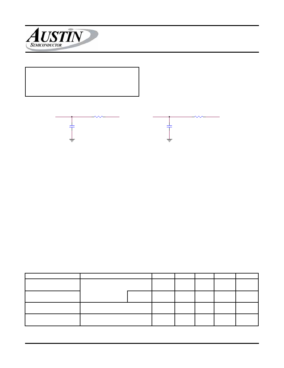
Fig. 1 Output Load Equivalent
Fig. 2 Output Load Equivalent
167 ohms
1.73V
C=5pF
C=30pF
Q
DATA RETENTION ELECTRICAL CHARACTERISTICS (L Version Only)
AC TEST CONDITIONS
Input pulse levels ................................................... Vss to 3.0V
Input rise and fall times ....................................................... 3ns
Input timing reference levels ............................................ 1.5V
Output reference levels ..................................................... 1.5V
Output load ............................................... See Figures 1 and 2
DESCRIPTION
SYMBOL
MIN
MAX
UNITS
NOTES
VCC for Retention Data
VDR
2V
Data Retention Current
(L Version Only)
VCC = 2V
ICCDR
4.5
mA
Chip Deselect to Data
Retention Time
tCDR
0ns
4
Operation Recovery Time
tR
10
ms
4, 11
CE\ > (Vcc -0.2V)
VIN > (Vcc -0.2V) or < 0.2V
CONDITIONS
相關PDF資料 |
PDF描述 |
|---|---|
| 5962-9579601HUA | DC-to-DC Voltage Converter |
| 5962-9579601HUC | High-Speed, Low-Voltage, 4 Ohm, Dual SPST CMOS Analog Switches |
| 5962-9579601HXA | DC-to-DC Voltage Converter |
| 5962-9579601HXC | DC-to-DC Voltage Converter |
| 5962-9579601HYA | High-Speed, Low-Voltage, 4 Ohm, Dual SPST CMOS Analog Switches |
相關代理商/技術參數(shù) |
參數(shù)描述 |
|---|---|
| 5962-9561328HUA | 制造商:Micross Components 功能描述:SRAM, 4MB - Trays |
| 5962-9561328HZA | 制造商:Micross Components 功能描述:SRAM, 4MB - Trays |
| 5962-9561329HUA | 制造商:Micross Components, Inc. 功能描述:SRAM, 4MB - Trays |
| 5962-9561329HZA | 制造商:Micross Components 功能描述:SRAM, 4MB - Trays |
| 5962-9561401QXA | 制造商:Texas Instruments 功能描述:Bus XCVR Dual 18-CH 3-ST 68-Pin CFPAK Tube 制造商:Rochester Electronics LLC 功能描述:- Bulk |
發(fā)布緊急采購,3分鐘左右您將得到回復。