- 您現(xiàn)在的位置:買賣IC網(wǎng) > PDF目錄371619 > 5962-97557 Hermetically Sealed Analog Isolation Amplifier(密封模擬隔離放大器) PDF資料下載
參數(shù)資料
| 型號: | 5962-97557 |
| 元件分類: | 運動控制電子 |
| 英文描述: | Hermetically Sealed Analog Isolation Amplifier(密封模擬隔離放大器) |
| 中文描述: | 密封的模擬隔離放大器(密封模擬隔離放大器) |
| 文件頁數(shù): | 13/16頁 |
| 文件大小: | 252K |
| 代理商: | 5962-97557 |
13
Applications Information
Functional Description
Figure 23 shows the primary
functional blocks of the HCPL-
7850. In operation, the sigma-
delta modulator converts the
analog input signal into a high-
speed serial bit stream. The time
average of this bit stream is
directly proportional to the input
signal. This stream of digital data
is encoded and optically
transmitted to the detector
circuit. The detected signal is
decoded and converted back into
an analog signal, which is filtered
to obtain the final output signal.
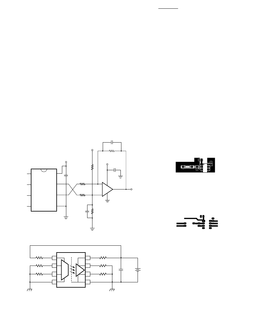
Figure 25. Single-Supply Post-Amplifier Circuit.
Figure 26. Top Layer of Printed
Circuit Board Layout.
Figure 27. Bottom Layer of a Printed
Circuit Board Layout.
Application Circuit
The recommended application
circuit is shown in Figure 24. A
floating power supply (which in
many applications could be the
same supply that is used to drive
the high-side power transistor) is
regulated to 5 V using a simple
three-terminal voltage regulator
(U1). The voltage from the
current sensing resistor, or shunt
(Rsense), is applied to the input
of the HCPL-7850 through an RC
anti-aliasing filter (R5, C3). And
finally, the differential output of
the isolation amplifier is
converted to a ground-referenced
single-ended output voltage with
a simple differential amplifier
circuit (U3 and associated
components). Although the
application circuit is relatively
simple, a few recommendations
should be followed to ensure
optimal performance.
Supplies and Bypassing
As mentioned above, an
inexpensive three-terminal
regulator can be used to reduce
the gate-drive power supply
voltage to 5 V. To help attenuate
high frequency power supply
noise or ripple, a resistor or
0.1 μF
+5 V
V
OUT
8
7
6
1
3
U2
5
2
4
R1
10.0 K
+5 V
C8
0.1 μF
–
+
MC34071
R3
10.0 K
HCPL-7850
C4
R4B
20.0 K
C6
150 pF
U3
R4A
20.0 K
+5 V
C5
150 pF
R2
10.0 K
C3
C2
C4
R5
TO R
SENSE+
TO R
SENSE–
TO V
DD1
TO V
DD2
V
OUT+
V
OUT–
Figure 28. Operating Circuit for Burn-In and Steady State Life Tests.
1
2
3
4
8
7
6
5
V
DD
V
IN+
V
IN–
GND
V
DD
V
OUT+
V
OUT–
GND
+
–
+
–
27
27
1 k
1 k
1 k
1 k
(+)
(–)
V
DD
5.5 V
DC
0.1 μF
CONDITIONS: I
CC
=17.5mA
T
A
=+125C
相關PDF資料 |
PDF描述 |
|---|---|
| 5962-9755801Q2A | High-Voltage PWM Power-Supply Controller |
| 5962-9755801QCA | Single 8-input NAND Gate |
| 5962-9756101Q2A | Triple 3-input AND Gate |
| 5962-9756101QCA | Triple 3-input AND Gate |
| 5962-9756201Q2A | Octal D-Type Flip-Flop |
相關代理商/技術參數(shù) |
參數(shù)描述 |
|---|---|
| 5962-9755701EPA | 功能描述:光隔離放大器 Hermetic Optocoupler RoHS:否 制造商:Avago Technologies 絕緣電壓:5000 Vrms 參考電壓: 電流傳遞比: 安裝風格:SMD/SMT 封裝 / 箱體:SOIC-8 封裝:Tube |
| 5962-9755701EPC | 功能描述:光隔離放大器 Hermetic Optocoupler RoHS:否 制造商:Avago Technologies 絕緣電壓:5000 Vrms 參考電壓: 電流傳遞比: 安裝風格:SMD/SMT 封裝 / 箱體:SOIC-8 封裝:Tube |
| 5962-9755701HPA | 功能描述:光隔離放大器 100kHz 1500Vdc Hermetically sealed RoHS:否 制造商:Avago Technologies 絕緣電壓:5000 Vrms 參考電壓: 電流傳遞比: 安裝風格:SMD/SMT 封裝 / 箱體:SOIC-8 封裝:Tube |
| 5962-9755701HPC | 功能描述:光隔離放大器 100kHz 1500Vdc Hermetically sealed RoHS:否 制造商:Avago Technologies 絕緣電壓:5000 Vrms 參考電壓: 電流傳遞比: 安裝風格:SMD/SMT 封裝 / 箱體:SOIC-8 封裝:Tube |
| 5962-9755701HXA | 功能描述:光隔離放大器 100kHz 1500Vdc Hermetically sealed RoHS:否 制造商:Avago Technologies 絕緣電壓:5000 Vrms 參考電壓: 電流傳遞比: 安裝風格:SMD/SMT 封裝 / 箱體:SOIC-8 封裝:Tube |
發(fā)布緊急采購,3分鐘左右您將得到回復。