- 您現(xiàn)在的位置:買賣IC網(wǎng) > PDF目錄369300 > 74ALVCH16831DBBRG4 (Texas Instruments, Inc.) 1-TO-4 ADDRESS REGISTER/DRIVER WITH 3-STATE OUTPUTS PDF資料下載
參數(shù)資料
| 型號(hào): | 74ALVCH16831DBBRG4 |
| 廠商: | Texas Instruments, Inc. |
| 英文描述: | 1-TO-4 ADDRESS REGISTER/DRIVER WITH 3-STATE OUTPUTS |
| 中文描述: | 1至4地址注冊(cè)/ 3驅(qū)動(dòng)態(tài)輸出 |
| 文件頁(yè)數(shù): | 1/9頁(yè) |
| 文件大小: | 130K |
| 代理商: | 74ALVCH16831DBBRG4 |

www.ti.com
FEATURES
Member of the Texas Instruments Widebus
Family
Bus Hold on Data Inputs Eliminates the Need
for External Pullup/Pulldown Resistors
Latch-Up Performance Exceeds 250 mA Per
JESD 17
ESD Protection Exceeds JESD 22
– 2000-V Human-Body Model (A114-A)
– 200-V Machine Model (A115-A)
– 1000-V Charged-Device Model (C101)
DESCRIPTION/ORDERING INFORMATION
This 1-bit to 4-bit address register/driver is designed
for 1.65-V to 3.6-V V
operation. The device is ideal
for use in applications in which a single address bus
is driving four separate memory locations. The
SN74ALVCH16831 can be used as a buffer or a
register, depending on the logic level of the select
(SEL) input.
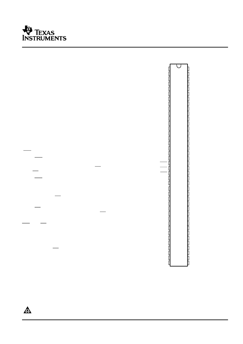
DBB PACKAGE
(TOP VIEW)
1
2
3
4
5
6
7
8
9
10
11
12
13
14
15
16
17
18
19
20
21
22
23
24
25
26
27
28
29
30
31
32
33
34
35
36
37
38
39
40
80
79
78
77
76
75
74
73
72
71
70
69
68
67
66
65
64
63
62
61
60
59
58
57
56
55
54
53
52
51
50
49
48
47
46
45
44
43
42
41
4Y1
3Y1
GND
2Y1
1Y1
V
CC
NC
A1
GND
NC
A2
GND
NC
A3
V
CC
NC
A4
GND
CLK
OE1
OE2
SEL
GND
A5
A6
V
CC
A7
NC
GND
A8
NC
GND
A9
NC
V
CC
4Y9
3Y9
GND
2Y9
1Y9
1Y2
2Y2
GND
3Y2
4Y2
V
CC
1Y3
2Y3
GND
3Y3
4Y3
GND
1Y4
2Y4
V
CC
3Y4
4Y4
GND
1Y5
2Y5
3Y5
4Y5
GND
1Y6
2Y6
V
CC
3Y6
4Y6
GND
1Y7
2Y7
GND
3Y7
4Y7
V
CC
1Y8
2Y8
GND
3Y8
4Y8
NC No internal connection
SN74ALVCH16831
1-TO-4 ADDRESS REGISTER/DRIVER
WITH 3-STATE OUTPUTS
SCES083F–AUGUST 1996–REVISED SEPTEMBER 2004
When SEL is logic high, the device is in the buffer
mode.
The
outputs
follow
controlled by the two output-enable (OE) controls.
Each OE controls two groups of nine outputs.
the
inputs
and
are
When SEL is logic low, the device is in the register
mode. The register is an edge-triggered D-type
flip-flop. On the positive transition of the clock (CLK)
input, data set up at the A inputs is stored in the
internal registers. OE controls operate the same as in
buffer mode.
When OE is logic low, the outputs are in a normal
logic state (high or low logic level). When OE is logic
high, the outputs are in the high-impedance state.
SEL and OE do not affect the internal operation of
the flip-flops. Old data can be retained or new data
can
be
entered
while
high-impedance state.
the
outputs
are
in
the
To ensure the high-impedance state during power up
or power down, OE should be tied to V
through a
pullup resistor; the minimum value of the resistor is
determined by the current-sinking capability of the
driver.
Active bus-hold circuitry holds unused or undriven
inputs at a valid logic state. Use of pullup or pulldown
resistors
with
the
bus-hold
recommended.
circuitry
is
not
Please be aware that an important notice concerning availability, standard warranty, and use in critical applications of Texas
Instruments semiconductor products and disclaimers thereto appears at the end of this data sheet.
Widebus is a trademark of Texas Instruments.
PRODUCTION DATA information is current as of publication date.
Products conform to specifications per the terms of the Texas
Instruments standard warranty. Production processing does not
necessarily include testing of all parameters.
Copyright 1996–2004, Texas Instruments Incorporated
相關(guān)PDF資料 |
PDF描述 |
|---|---|
| 74ALVCH16903DGVRE4 | 3.3-V 12-BIT UNIVERSAL BUS DRIVER WITH PARITY CHECKER AND DUAL 3-STATE OUTPUTS |
| 74ALVCH16903DLRG4 | 3.3-V 12-BIT UNIVERSAL BUS DRIVER WITH PARITY CHECKER AND DUAL 3-STATE OUTPUTS |
| 74ALVCH16973DLRG4 | 8-BIT BUS TRANSCEIVER AND TRANSPARENT D-TYPE LATCH WITH FOUR INDEPENDENT BUFFERS |
| 74ALVCH32245 | 32-BIT BUS TRANSCEIVER WITH 3-STATE OUTPUTS |
| 74ALVCHR16269AVRE4 | 12-BIT TO 24-BIT REGISTERED BUS EXCHANGER WITH 3-STATE OUTPUTS |
相關(guān)代理商/技術(shù)參數(shù) |
參數(shù)描述 |
|---|---|
| 74ALVCH16832 | 制造商:PHILIPS 制造商全稱:NXP Semiconductors 功能描述:7-bit to 28-bit address register/driver with 3-state outputs |
| 74ALVCH16832DGG | 制造商:PHILIPS 制造商全稱:NXP Semiconductors 功能描述:7-bit to 28-bit address register/driver with 3-state outputs |
| 74ALVCH16832DGG,11 | 功能描述:寄存器 1TO4BIT ADDRES DRV RoHS:否 制造商:NXP Semiconductors 邏輯類型:CMOS 邏輯系列:HC 電路數(shù)量:1 最大時(shí)鐘頻率:36 MHz 傳播延遲時(shí)間: 高電平輸出電流:- 7.8 mA 低電平輸出電流:7.8 mA 電源電壓-最大:6 V 最大工作溫度:+ 125 C 封裝 / 箱體:SOT-38 封裝:Tube |
| 74ALVCH16832DGG,112 | 制造商:NXP Semiconductors 功能描述: |
| 74ALVCH16832DGG,118 | 制造商:NXP Semiconductors 功能描述: |
發(fā)布緊急采購(gòu),3分鐘左右您將得到回復(fù)。