- 您現(xiàn)在的位置:買賣IC網(wǎng) > PDF目錄369304 > 74FCT162H501CTPVCT (Texas Instruments, Inc.) 18-Bit Registered Transceivers PDF資料下載
參數(shù)資料
| 型號: | 74FCT162H501CTPVCT |
| 廠商: | Texas Instruments, Inc. |
| 元件分類: | 通用總線功能 |
| 英文描述: | 18-Bit Registered Transceivers |
| 中文描述: | 18位注冊收發(fā)器 |
| 文件頁數(shù): | 1/8頁 |
| 文件大小: | 66K |
| 代理商: | 74FCT162H501CTPVCT |

18-Bit Registered Transceivers
CY74FCT16501T
CY74FCT162501T
CY74FCT162H501T
SCCS057 - August 1994 - Revised March 2000
Data sheet acquired from Cypress Semiconductor Corporation.
Data sheet modified to remove devices not offered.
Copyright
2000, Texas Instruments Incorporated
1CY74FCT162H501
T
Features
FCT-E speed at 3.8 ns
Power-off disable outputs permits live insertion
Edge-rate control circuitry for significantly improved
noise characteristics
Typical output skew < 250 ps
ESD > 2000V
TSSOP (19.6 mil pitch) and SSOP (25-mil pitch)
packages
Industrial temperature range of
40C to +85C
V
CC
= 5V
±
10%
CY74FCT16501T Features:
64 mA sink current, 32 mA source current
Typical V
OLP
(ground bounce) <1.0V at V
CC
= 5V,
T
A
= 25C
CY74FCT162501T Features:
Balanced 24 mA output drivers
Reduced system switching noise
Typical V
OLP
(ground bounce) <0.6V at V
CC
= 5V,
T
A
= 25C
CY74FCT162H501T Features:
Bus hold retains last active state
Eliminates the need for external pull-up or pull-down
resistors
Functional Description
These 18-bit universal bus transceivers can be operated in
transparent, latched or clock modes by combining D-type
latches and D-type flip-flops. Data flow in each direction is
controlled by output enable (OEAB and OEBA), latch enable
(LEAB and LEBA), and clock inputs (CLKAB and CLKBA). For
A-to-B data flow, the device operates in transparent mode
when LEAB is HIGH. When LEAB is LOW, the A data is latched
if CLKAB is held at a HIGH or LOW logic level. If LEAB is LOW,
the A bus data is stored in the latch/flip-flop on the
LOW-to-HIGH transition of CLKAB. OEAB performs the output
enable function on the B port. Data flow from B-to-A is similar
to that of A-to-B and is controlled by OEBA, LEBA, and CLKBA.
The output buffers are designed with a power-off disable
feature to allow live insertion of boards.
The
CY74FCT16501T
is
high-capacitance loads and low-impedance backplanes.
THE CY74FCT162501T has 24-mA balanced output drivers
with current limiting resistors in the outputs. This reduces the
need for external terminating resistors and provides for minimal
undershoot
and
reduced
CY74FCT162501T is ideal for driving transmission lines.
The CY74FCT162H501T is a 24-mA balanced output part, that
has “bus hold” on the data inputs. The device retains the input’s
last state whenever the input goes to high impedance. This
eliminates the need for pull-up/down resistors and prevents
floating inputs.
ideally
suited
for
driving
ground
bounce.
The
GND
B
7
B
8
B
9
B
10
B
11
B
12
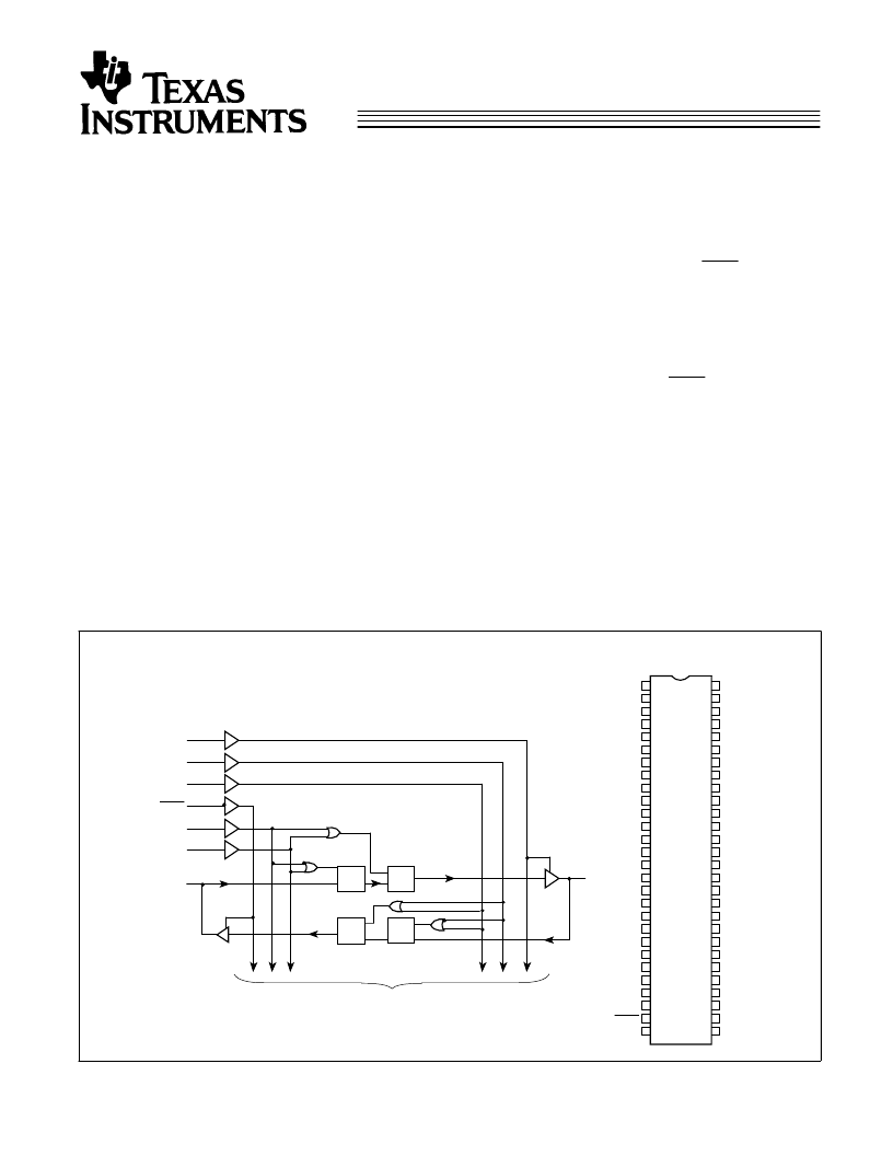
Functional Block Diagram
Pin Configuration
SSOP/TSSOP
Top View
1
2
3
4
5
6
7
8
9
10
11
12
13
14
15
16
17
18
19
20
21
22
23
24
25
26
27
28
OEAB
LEAB
A
1
GND
A
2
A
3
GND
B
13
B
14
B
15
V
CC
B
16
B
17
V
CC
A
4
A
5
A
6
GND
GND
B
18
CLKBA
GND
A
13
A
14
A
15
FCT16501-1
A
7
A
8
A
9
A
10
A
11
A
12
GND
A
18
OEBA
LEBA
V
CC
A
16
A
17
56
55
54
53
52
51
50
49
48
47
46
45
44
43
42
41
40
39
38
37
36
35
34
33
32
31
30
29
GND
CLKAB
B
1
GND
B
2
B
3
V
CC
B
4
B
5
B
6
GND
OEAB
CLKBA
LEBA
OEBA
CLKAB
LEAB
C
D
C
D
C
D
A
1
B
1
C
D
TO 17 OTHER CHANNELS
FCT16501-2
相關(guān)PDF資料 |
PDF描述 |
|---|---|
| 74FCT162646ETPACT | 16-Bit Registered Transceivers |
| 74FCT162646ETPVCT | 16-Bit Registered Transceivers |
| 74FCT162652CTPVCT | 16-Bit Registered Transceivers |
| 74FCT162823 | 18-Bit Registers |
| 74FCT162823ATPACT | 18-Bit Registers |
相關(guān)代理商/技術(shù)參數(shù) |
參數(shù)描述 |
|---|---|
| 74FCT162H501ETPACT | 制造商:TI 制造商全稱:Texas Instruments 功能描述:18-Bit Registered Transceivers |
| 74FCT162H501ETPVC | 制造商:Rochester Electronics LLC 功能描述:- Bulk 制造商:Texas Instruments 功能描述: |
| 74FCT162H501ETPVCT | 制造商:TI 制造商全稱:Texas Instruments 功能描述:18-Bit Registered Transceivers |
| 74FCT162H543CTPACT | 功能描述:總線收發(fā)器 16B Reg Transceivers RoHS:否 制造商:Fairchild Semiconductor 邏輯類型:CMOS 邏輯系列:74VCX 每芯片的通道數(shù)量:16 輸入電平:CMOS 輸出電平:CMOS 輸出類型:3-State 高電平輸出電流:- 24 mA 低電平輸出電流:24 mA 傳播延遲時間:6.2 ns 電源電壓-最大:2.7 V, 3.6 V 電源電壓-最小:1.65 V, 2.3 V 最大工作溫度:+ 85 C 封裝 / 箱體:TSSOP-48 封裝:Reel |
| 74FCT162H952ATPACT | 功能描述:總線收發(fā)器 16B Reg Transceivers RoHS:否 制造商:Fairchild Semiconductor 邏輯類型:CMOS 邏輯系列:74VCX 每芯片的通道數(shù)量:16 輸入電平:CMOS 輸出電平:CMOS 輸出類型:3-State 高電平輸出電流:- 24 mA 低電平輸出電流:24 mA 傳播延遲時間:6.2 ns 電源電壓-最大:2.7 V, 3.6 V 電源電壓-最小:1.65 V, 2.3 V 最大工作溫度:+ 85 C 封裝 / 箱體:TSSOP-48 封裝:Reel |
發(fā)布緊急采購,3分鐘左右您將得到回復(fù)。