- 您現(xiàn)在的位置:買賣IC網(wǎng) > PDF目錄369314 > 74LS173 (Motorola, Inc.) 4-BIT D-TYPE REGISTER WITH 3-STATE OUTPUTS PDF資料下載
參數(shù)資料
| 型號: | 74LS173 |
| 廠商: | Motorola, Inc. |
| 英文描述: | 4-BIT D-TYPE REGISTER WITH 3-STATE OUTPUTS |
| 中文描述: | 4位D型登記注冊三態(tài)輸出 |
| 文件頁數(shù): | 5/19頁 |
| 文件大小: | 562K |
| 代理商: | 74LS173 |

SN54173, SN54LS173A, SN74173, SN74LS173A
4-BIT D-TYPE REGISTERS
WITH 3-STATE OUTPUTS
SDLS067A – OCTOBER 1976 – REVISED JUNE 1999
5
POST OFFICE BOX 655303
DALLAS, TEXAS 75265
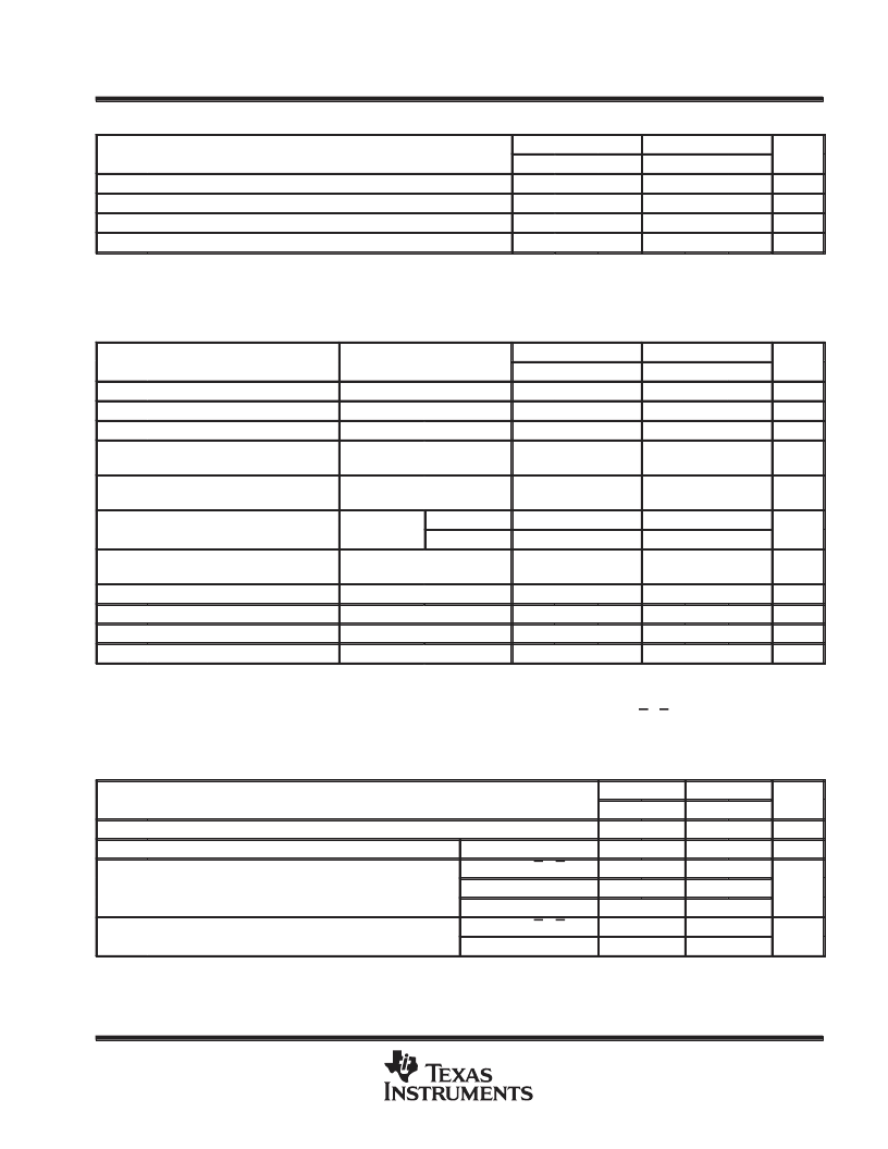
recommended operating conditions (see Note 3)
SN54173
NOM
SN74173
NOM
UNIT
MIN
MAX
MIN
MAX
VCC
IOH
IOL
TA
NOTE 3: All unused inputs of the device must be held at VCC or GND to ensure proper device operation. Refer to the TI application report,
Implications of Slow or Floating CMOS Inputs,literature number SCBA004.
Supply voltage
4.5
5
5.5
4.75
5
5.25
V
High-level output current
–2
–5.2
mA
Low-level output current
16
16
mA
°
C
Operating free-air temperature
–55
125
0
70
electrical characteristics over recommended operating free-air temperature range (unless
otherwise noted)
PARAMETER
TEST CONDITIONS
SN54173
TYP
SN74173
TYP
UNIT
MIN
MAX
MIN
MAX
VIH
VIL
VIK
High-level input voltage
2
2
V
Low-level input voltage
0.8
0.8
V
Input clamp voltage
VCC = MIN,
VCC = MIN,
VIL = 0.8 V,
VCC = MIN,
VIL = 0.8 V,
II = –12 mA
VIH = 2 V,
IOH = MAX
VIH = 2 V,
IOL = 16 mA
VO = 2.4 V
VO = 0.4 V
–1.5
–1.5
V
VOH
High-level output voltage
2.4
2.4
V
VOL
Low-level output voltage
0.4
0.4
V
IO( ff)
IO(off)
Off-state (high-impedance state)
( g
output current
VCC = MAX,
VIH = 2 V
150
40
μ
A
–150
–40
II
Input current
at maximum input voltage
VCC = MAX,
VI = 5.5 V
1
1
mA
IIH
IIL
IOS
ICC
For conditions shown as MIN or MAX, use the appropriate value specified under recommended operating conditions.
All typical values are at VCC = 5 V, TA = 25
°
C.
§Not more than one output should be shorted at a time.
NOTE 4: ICC is measured with all outputs open; CLR grounded, following momentary connection to 4.5 V, N, G1, G2, and all data inputs grounded;
and CLK and M at 4.5 V.
High-level input current
VCC = MAX,
VCC = MAX,
VCC = MAX
VCC = MAX,
VI = 2.4 V
VI = 0.4 V
40
40
μ
A
mA
Low-level input current
Short-circuit output current§
–1.6
–1.6
–30
–70
–30
–70
mA
Supply current
See Note 4
50
72
50
72
mA
timing requirements over recommended operating conditions (unless otherwise noted)
SN54173
MIN
SN74173
MIN
UNIT
MAX
MAX
fclock
tw
Input clock frequency
25
25
MHz
Pulse duration
CLK or CLR
20
20
ns
Data enable (G1, G2)
17
17
tsu
Setup time
Data
10
10
ns
CLR (inactive state)
10
10
th
Hold time
Data enable (G1, G2)
Data
2
2
ns
10
10
相關(guān)PDF資料 |
PDF描述 |
|---|---|
| 74LS174 | Hex/Quadruple D-type Flip-Flips(with clear) |
| 74LS175 | Hex/Quadruple D-type Flip-Flips(with clear) |
| 74LS174 | LOW POWER SCHOTTKY |
| 74LS175 | LOW POWER SCHOTTKY |
| 74LS174 | Hex/Quad D Flip-Flops with Clear |
相關(guān)代理商/技術(shù)參數(shù) |
參數(shù)描述 |
|---|---|
| 74LS173A | 制造商:Semiconductors 功能描述: |
| 74LS173DC | 制造商:未知廠家 制造商全稱:未知廠家 功能描述:Quad D-Type Flip-Flop |
| 74LS173PC | 制造商:Rochester Electronics LLC 功能描述:- Bulk |
| 74LS173SC | 制造商:Rochester Electronics LLC 功能描述:- Bulk |
| 74LS174 | 制造商:NTE Electronics 功能描述: 制造商:Semiconductors 功能描述: |
發(fā)布緊急采購,3分鐘左右您將得到回復(fù)。