- 您現在的位置:買賣IC網 > PDF目錄24776 > 933748630652 (NXP SEMICONDUCTORS) HCT SERIES, QUAD 2-INPUT NAND GATE, PDIP14 PDF資料下載
參數資料
| 型號: | 933748630652 |
| 廠商: | NXP SEMICONDUCTORS |
| 元件分類: | 門電路 |
| 英文描述: | HCT SERIES, QUAD 2-INPUT NAND GATE, PDIP14 |
| 封裝: | SOT-27-1, DIP-14 |
| 文件頁數: | 5/12頁 |
| 文件大小: | 142K |
| 代理商: | 933748630652 |

December 1990
2
Philips Semiconductors
Product specication
Quad 2-input NAND gate
74HC/HCT03
FEATURES
Level shift capability
Output capability: standard (open drain)
ICC category: SSI
GENERAL DESCRIPTION
The 74HC/HCT03 are high-speed Si-gate CMOS devices
and are pin compatible with low power Schottky TTL
(LSTTL). They are specified in compliance with JEDEC
standard no. 7A.
The 74HC/HCT03 provide the 2-input NAND function.
The 74HC/HCT03 have open-drain N-transistor outputs,
which are not clamped by a diode connected to VCC. In
the OFF-state, i.e. when one input is LOW, the output
may be pulled to any voltage between GND and VOmax.
This allows the device to be used as a LOW-to-HIGH or
HIGH-to-LOW level shifter. For digital operation and
OR-tied output applications, these devices must have a
pull-up resistor to establish a logic HIGH level.
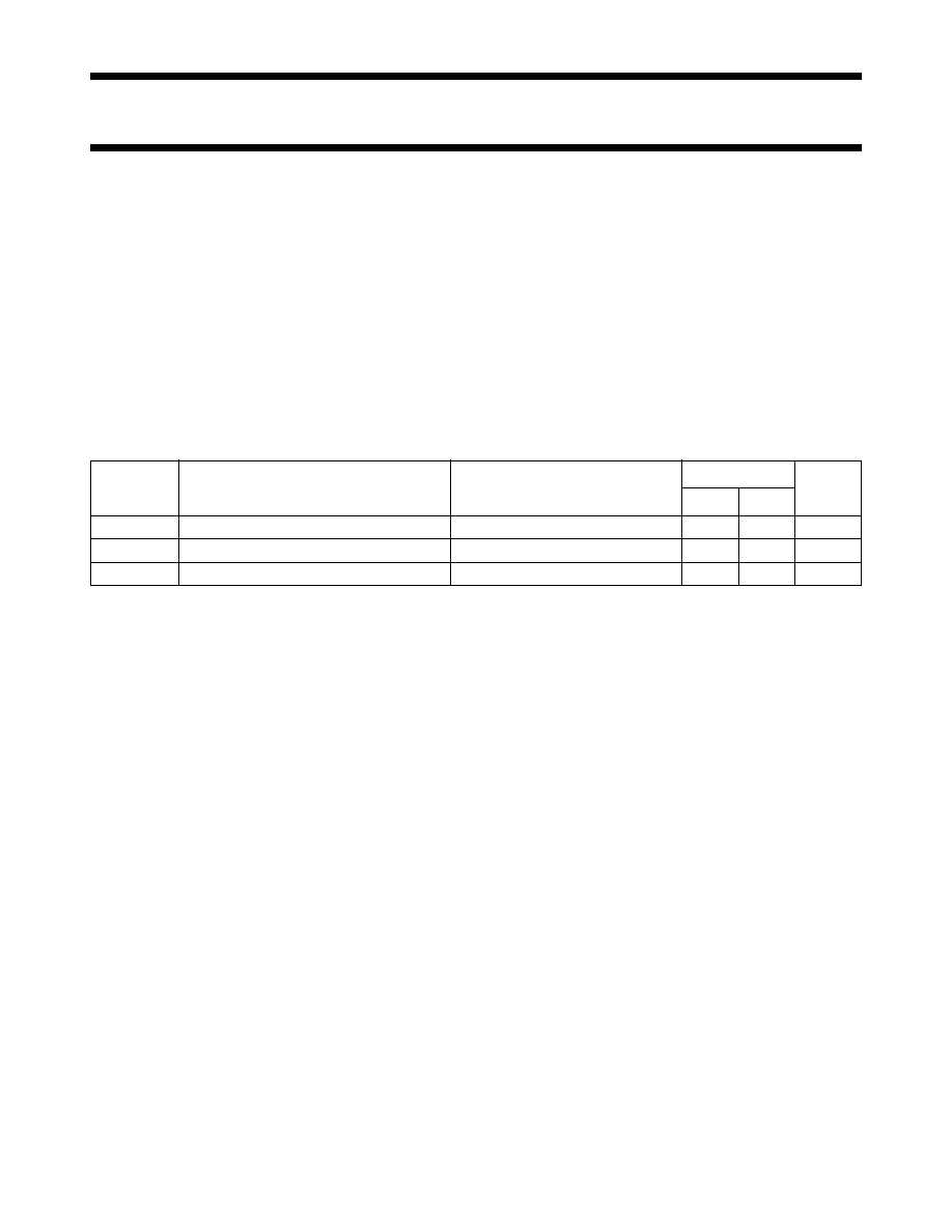
QUICK REFERENCE DATA
GND = 0 V; Tamb =25 °C; tr =tf = 6 ns
Notes
1. CPD is used to determine the dynamic power dissipation (PD in W):
PD =CPD × VCC2× fi + ∑ (CL × VCC2 × fo) + ∑ (VO2/RL) × duty factor LOW, where:
fi = input frequency in MHz
fo = output frequency in MHz
VO = output voltage in V
CL = output load capacitance in pF
VCC = supply voltage in V
RL = pull-up resistor in M
∑ (CL × VCC2 × fo) = sum of outputs
∑ (VO2/RL) = sum of outputs
2. For HC the condition is VI = GND to VCC
For HCT the condition is VI = GND to VCC 1.5 V
3. The given value of CPD is obtained with:
CL = 0 pF and RL = ∞
ORDERING INFORMATION
See
“74HC/HCT/HCU/HCMOS Logic Package Information”.
SYMBOL
PARAMETER
CONDITIONS
TYPICAL
UNIT
HC
HCT
tPZL/ tPLZ
propagation delay
CL = 15 pF; RL =1 k; VCC = 5 V 8
10
ns
CI
input capacitance
3.5
pF
CPD
power dissipation capacitance per gate
notes 1, 2 and 3
4.0
pF
相關PDF資料 |
PDF描述 |
|---|---|
| 935173760118 | HCT SERIES, QUAD 2-INPUT NAND GATE, PDSO14 |
| 935174180118 | HC/UH SERIES, QUAD 2-INPUT NAND GATE, PDSO14 |
| 933748660652 | HC/UH SERIES, QUAD 2-INPUT NAND GATE, PDSO14 |
| 933748640653 | HCT SERIES, QUAD 2-INPUT NAND GATE, PDSO14 |
| 935174270112 | HC/UH SERIES, QUAD 2-INPUT AND GATE, PDSO14 |
相關代理商/技術參數 |
參數描述 |
|---|---|
| 93378-003 | 制造商:FCI 功能描述:MEMORY CARD RECEPTACLE - Bulk |
| 9337-A17R | 制造商:GC Electronics 功能描述: |
| 9337C | 制造商:Hubbell Premise Wiring 功能描述: |
| 9337-CHR-100 | 制造商:Belden Inc 功能描述: |
| 9337CKE100M | 制造商:RFMD 制造商全稱:RF Micro Devices 功能描述:380W GaN WIDEBAND PULSED |
發(fā)布緊急采購,3分鐘左右您將得到回復。