- 您現(xiàn)在的位置:買賣IC網(wǎng) > PDF目錄24705 > 934056334135 (NXP SEMICONDUCTORS) 2 CHANNEL, UHF BAND, Si, N-CHANNEL, RF SMALL SIGNAL, MOSFET PDF資料下載
參數(shù)資料
| 型號: | 934056334135 |
| 廠商: | NXP SEMICONDUCTORS |
| 元件分類: | 小信號晶體管 |
| 英文描述: | 2 CHANNEL, UHF BAND, Si, N-CHANNEL, RF SMALL SIGNAL, MOSFET |
| 封裝: | PLASTIC, SMD, UMT6, SC-88, 6 PIN |
| 文件頁數(shù): | 5/12頁 |
| 文件大小: | 103K |
| 代理商: | 934056334135 |

2001 Apr 25
2
Philips Semiconductors
Product specication
Dual N-channel dual gate MOS-FET
BF1204
FEATURES
Two low noise gain controlled amplifiers in a single
package
Superior cross-modulation performance during AGC
High forward transfer admittance
High forward transfer admittance to input capacitance
ratio.
APPLICATIONS
Gain controlled low noise amplifiers for VHF and UHF
applications with 3 to 9 V supply voltage, such as digital
and analog television tuners and professional
communications equipment.
DESCRIPTION
The BF1204 is a combination of two equal dual gate
MOS-FET amplifiers with shared source and gate 2 leads.
The source and substrate are interconnected. Internal bias
circuits enable DC stabilization and a very good
cross-modulation performance during AGC. Integrated
diodes between the gates and source protect against
excessive input voltage surges. The transistor has a
SOT363 micro-miniature plastic package.
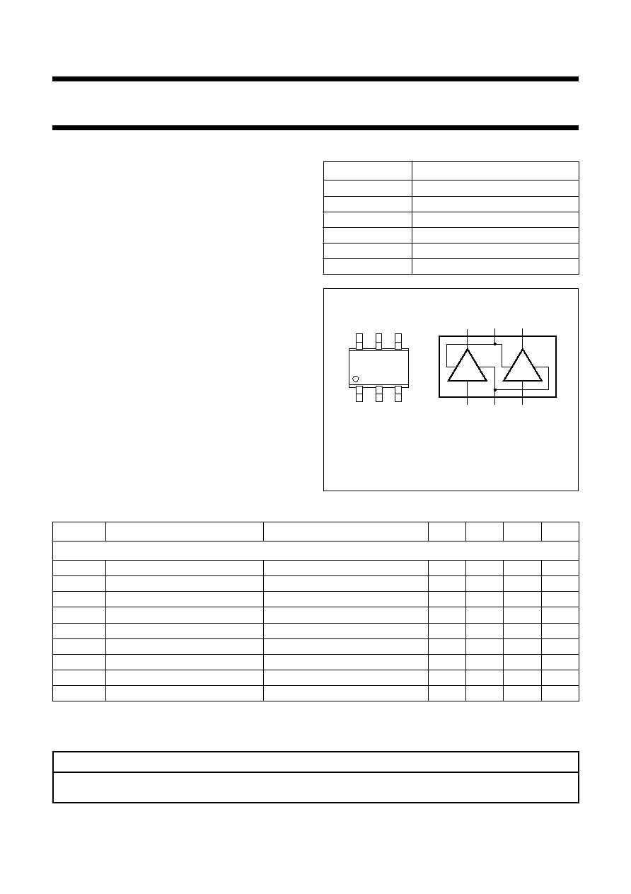
PINNING - SOT363
PIN
DESCRIPTION
1
gate 1 (a)
2
gate 2
3
gate 1 (b)
4
drain (b)
5
source
6
drain (a)
handbook, halfpage
MBL252
AMP
a
AMP
b
d (a)
s
d (b)
g1 (a)
Top view
g2
g1 (b)
13
2
4
5
6
Fig.1 Simplified outline and symbol.
Marking code: L3-
QUICK REFERENCE DATA
Note
1. Ts is the temperature at the soldering point of the source lead.
SYMBOL
PARAMETER
CONDITIONS
MIN.
TYP.
MAX.
UNIT
Per MOS-FET; unless otherwise specied
VDS
drain-source voltage
10
V
ID
drain current (DC)
30
mA
Ptot
total power dissipation
Ts ≤ 102 °C; note 1
200
mW
y
fs
forward transfer admittance
ID = 12 mA; f = 1 MHz
25
30
40
mS
Cig1-s
input capacitance at gate 1
ID = 12 mA; f = 1 MHz
1.7
2.2
pF
Crss
reverse transfer capacitance
f = 1 MHz
15
fF
NF
noise gure
f = 800 MHz
1.1
1.8
dB
Xmod
cross-modulation
input level for k = 1% at 40 dB AGC 100
105
dB
V
Tj
operating junction temperature
150
°C
CAUTION
This product is supplied in anti-static packing to prevent damage caused by electrostatic discharge during transport
and handling. For further information, refer to Philips specs.: SNW-EQ-608, SNW-FQ-302A and SNW-FQ-302B.
相關PDF資料 |
PDF描述 |
|---|---|
| 06035C332KAT2A | KONDENSATOR 3.3NF 50V 10ST |
| 934056335118 | 12 A BUF OR INV BASED PRPHL DRVR, PSSO2 |
| 0402YY103K2700J | KONDENSATOR 10NF 16V 10ST |
| 06033C103KAT2A | KONDENSATOR 10NF 50V 10ST |
| 06033C223KAT2A | KONDENSATOR 22NF 25V 10ST |
相關代理商/技術(shù)參數(shù) |
參數(shù)描述 |
|---|---|
| 934056947115 | 制造商:NXP Semiconductors 功能描述:Trans GP BJT NPN 15V 0.2A 4-Pin(3+Tab) SOT-89 T/R |
| 934056954118 | 制造商:NXP Semiconductors 功能描述:Trans MOSFET N-CH 60V 34A 3-Pin(2+Tab) D2PAK T/R |
| 934057052116 | 制造商:PHILIPS 制造商全稱:NXP Semiconductors 功能描述:Logic level four-quadrant triac |
| 934057052126 | 制造商:PHILIPS 制造商全稱:NXP Semiconductors 功能描述:Logic level four-quadrant triac |
| 934057052412 | 制造商:PHILIPS 制造商全稱:NXP Semiconductors 功能描述:Logic level four-quadrant triac |
發(fā)布緊急采購,3分鐘左右您將得到回復。