- 您現(xiàn)在的位置:買賣IC網(wǎng) > PDF目錄36334 > 935240230112 (NXP SEMICONDUCTORS) VERTICAL DEFLECTION IC, PZIP13 PDF資料下載
參數(shù)資料
| 型號(hào): | 935240230112 |
| 廠商: | NXP SEMICONDUCTORS |
| 元件分類: | 偏轉(zhuǎn) |
| 英文描述: | VERTICAL DEFLECTION IC, PZIP13 |
| 封裝: | POWER, PLASTIC, SOT-141-6, DIL-BENT-SIL, 13 PIN |
| 文件頁數(shù): | 13/18頁 |
| 文件大?。?/td> | 154K |
| 代理商: | 935240230112 |
1998 Sep 03
4
Philips Semiconductors
Preliminary specication
Full bridge current driven vertical deection
output circuit in LVDMOS
TDA8354Q
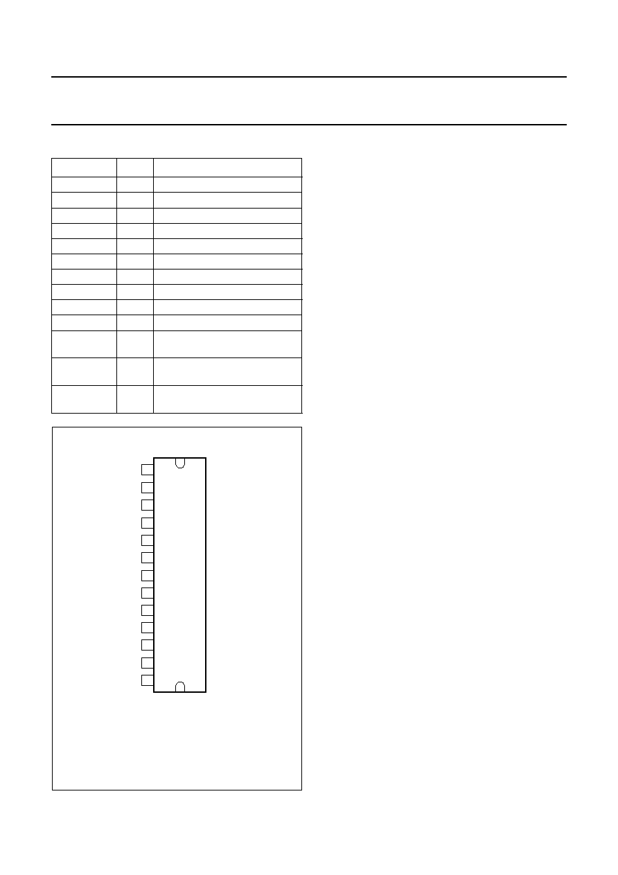
PINNING
SYMBOL
PIN
DESCRIPTION
Vo(guard)
1
guard output voltage
Vi(M)
2
measuring resistor input
Vi(con)
3
conversion resistor input
VP(B)
4
supply voltage B
Vo(B)
5
output voltage B
GNDB
6
ground B
Vb
7
yback supply voltage
GNDA
8
ground A
Vo(A)
9
output voltage A
VP(A)
10
supply voltage A
Ii(neg)
11
input power-stage (negative);
includes Ii(bias) signal bias
Ii(pos)
12
input power-stage (positive);
includes Ii(bias) signal bias
Ii(comp)
13
damping resistor compensation
current input
Fig.2 Pin configuration.
The die has been glued to the metal block of the package. If the metal
block is not insulated from the heat sink, the heat sink may only be
connected directly to pins 6 and 8.
handbook, halfpage
TDA8354Q
MGL462
1
2
3
4
5
6
7
8
9
10
11
12
13
Vo(guard)
Vi(M)
Vi(con)
VP(B)
Vo(B)
GNDB
Vflb
GNDA
Vo(A)
VP(A)
Ii(neg)
Ii(pos)
Ii(comp)
FUNCTIONAL DESCRIPTION
The vertical driver circuit is a bridge configuration.
The deflection coil is connected between the output
amplifiers, which are driven in phase opposition.
The differential input circuit is current driven. The input
circuit is special intended for direct connection to driver
circuits which deliver symmetrical current signals, but is
also suitable for asymmetrical currents. The current to
voltage conversion is done by the external resistor (Rcon)
connected between the output of the input conversion
stage and output stage B. This voltage is compared with
the output current through the deflection coil measured as
voltage across RM, which provides internal feedback
information. The relationship between the differential input
current and the output current is defined by:
2
× Ii(diff) × Rcon =Icoil × RM The output current is
adjustable from 0.5 A (p-p) to 3.2 A (p-p) by varying Rcon.
The maximum input current is 800
A peak for each pin.
The minimum input current should be 50
A.
Flyback supply
The flyback voltage is determined by an additional supply
voltage Vflb. The principle of operating with two supply
voltages (class G) makes it possible to fix the supply
voltage VP optimum for the scan voltage and the second
supply voltage Vflb optimum for the flyback voltage. Using
this method, very high efficiency is achieved. The supply
voltage Vflb is almost totally available as flyback voltage
across the coil, this being possible due to the absence of a
coupling capacitor (not necessary, due to the bridge
configuration). The very short rise and fall time of the
flyback switch is >400 V/
s.
Protection
The output circuit has protection circuits for:
Die temperature control
Overvoltage of output stage A.
相關(guān)PDF資料 |
PDF描述 |
|---|---|
| 935264151112 | VERTICAL DEFLECTION IC, PZIP13 |
| 935242210551 | SPECIALTY CONSUMER CIRCUIT, PQFP160 |
| 935242210557 | SPECIALTY CONSUMER CIRCUIT, PQFP160 |
| 935262922551 | SPECIALTY CONSUMER CIRCUIT, PQFP160 |
| 935262922557 | SPECIALTY CONSUMER CIRCUIT, PQFP160 |
相關(guān)代理商/技術(shù)參數(shù) |
參數(shù)描述 |
|---|---|
| 935241-0001 | 制造商: 功能描述: 制造商:DIGITRAN 功能描述: 制造商:undefined 功能描述: |
| 935241-1 | 制造商:DIGITRAN 功能描述: 制造商:DTRAN 功能描述: |
| 935245650125 | 制造商:NXP Semiconductors 功能描述:Inverter 1-Element CMOS 5-Pin TSSOP T/R |
| 935248-90 | 制造商:JANCO 功能描述:935248-90 |
| 9-3525-012 | 制造商:KEYSTONE 功能描述:MODIFIED 3525,VERSION E |
發(fā)布緊急采購,3分鐘左右您將得到回復(fù)。