- 您現(xiàn)在的位置:買賣IC網(wǎng) > PDF目錄24826 > 935263261557 (NXP SEMICONDUCTORS) 8-BIT, MROM, 16 MHz, MICROCONTROLLER, PQFP80 PDF資料下載
參數(shù)資料
| 型號: | 935263261557 |
| 廠商: | NXP SEMICONDUCTORS |
| 元件分類: | 微控制器/微處理器 |
| 英文描述: | 8-BIT, MROM, 16 MHz, MICROCONTROLLER, PQFP80 |
| 封裝: | PLASTIC, QFP-80 |
| 文件頁數(shù): | 6/76頁 |
| 文件大小: | 567K |
| 代理商: | 935263261557 |
第1頁第2頁第3頁第4頁第5頁當(dāng)前第6頁第7頁第8頁第9頁第10頁第11頁第12頁第13頁第14頁第15頁第16頁第17頁第18頁第19頁第20頁第21頁第22頁第23頁第24頁第25頁第26頁第27頁第28頁第29頁第30頁第31頁第32頁第33頁第34頁第35頁第36頁第37頁第38頁第39頁第40頁第41頁第42頁第43頁第44頁第45頁第46頁第47頁第48頁第49頁第50頁第51頁第52頁第53頁第54頁第55頁第56頁第57頁第58頁第59頁第60頁第61頁第62頁第63頁第64頁第65頁第66頁第67頁第68頁第69頁第70頁第71頁第72頁第73頁第74頁第75頁第76頁

Philips Semiconductors
Product specification
P83C557E4/P80C557E4/P89C557E4
Single-chip 8-bit microcontroller
1999 Mar 02
14
6.4
I/O Facilities
The P8xC557E4 has six 8-bit ports. Ports 0 to 3 are the same as in
the 80C51, with the exception of the additional functions of Port 1.
The parallel I/O function of Port 4 is equal to that of Ports 1, 2 and 3.
Port 5 has a parallel input port function, but has no function as an
output port.
The SDA and SCL lines serve the serial port SIO1 (I2C). Because
the I2C-bus may be active while the device is disconnected from
VDD, these pins, are provided with open drain drivers.
Ports 0, 1, 2, 3, 4 and 5 perform the following alternative functions:
Port 0 :
provides the multiplexed low-order address and data
bus used for expanding the P8xC557E4 with standard
memories and peripherals.
Port 1 :
Port 1 is used for a number of special functions:
4 capture inputs (or external interrupt request inputs if
capture information is not utilized)
– external counter input
– external counter reset input
Port 2 :
provides the high-order address bus when the
P8xC557E4 is expanded with external Program
Memory and/or external Data Memory.
Port 3 :
pins can be configured individually to provide:
– external interrupt request inputs
– counter inputs
– receiver input and transmitter output of seri port
SIO 0 (UART)
– control signals to read and write external Data
Memory
Port 4 :
can be configured to provide signals indicating a match
between timer counter T2 and its compare registers.
Port 5 :
may be used in conjunction with the ADC interface.
Unused analog inputs can be used as digital inputs. As
Port 5 lines may be used as inputs to the ADC, these
digital inputs have an inherent hysteresis to prevent the
input logic from drawing too much current from the
power lines when driven by analog signals. Channel to
channel crosstalk should be taken into consideration
when both digital and analog signals are simultaneously
input to Port 5 (see DC characteristics).
All ports are bidirectional with the exception of Port 5 which is an
input port.
Pins of which the alternative function is not used may be used as
normal bidirectional I/Os.
The generation or use of a Port 1, Port 3 or Port 4 pin as an
alternative function is carried out automatically by the P8xC557E4
provided the associated Special Function Register bit is set HIGH.
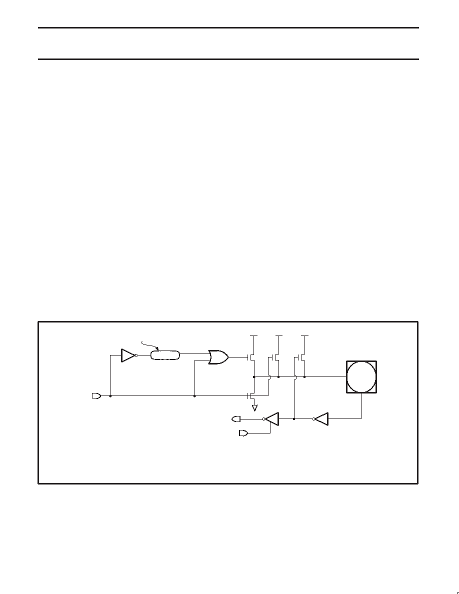
The pull-up arrangements of Ports 1 – 4 are shown in Figure 9.
Figure 9. I/O buffers in the P8xC557E4 (Ports 1, 2, 3 and 4)
VDD
QN
2 System Clock Periods
Port
Pin
n
From Port
Latch
VDD
P1
P2
P3
Input Data
Read Port Pin
P1 is turned on for 2 system clock periods after QN makes a 1-to-0 transition.
During this time, P1 also turns on P3 through the inverter to form an additional pull up.
相關(guān)PDF資料 |
PDF描述 |
|---|---|
| 935263206557 | 8-BIT, MROM, 16 MHz, MICROCONTROLLER, PQFP80 |
| 935268065557 | 8-BIT, MROM, 16 MHz, MICROCONTROLLER, PQFP80 |
| 935263263557 | 8-BIT, MROM, 16 MHz, MICROCONTROLLER, PQFP80 |
| 935263262557 | 8-BIT, MROM, 16 MHz, MICROCONTROLLER, PQFP80 |
| 935263208557 | 8-BIT, MROM, 16 MHz, MICROCONTROLLER, PQFP80 |
相關(guān)代理商/技術(shù)參數(shù) |
參數(shù)描述 |
|---|---|
| 935264217557 | 制造商:NXP Semiconductors 功能描述:SUB ONLY IC |
| 935267356112 | 制造商:NXP Semiconductors 功能描述:IC TEA1507PN |
| 935268081112 | 制造商:NXP Semiconductors 功能描述:SUB ONLY IC |
| 935268721125 | 制造商:NXP Semiconductors 功能描述:Buffer/Line Driver 1-CH Non-Inverting 3-ST CMOS 5-Pin TSSOP T/R |
| 935269304128 | 制造商:ST-Ericsson 功能描述:IC AUDIO CODEC W/TCH SCRN 48LQFP |
發(fā)布緊急采購,3分鐘左右您將得到回復(fù)。