- 您現(xiàn)在的位置:買賣IC網(wǎng) > PDF目錄360618 > 93AA56AP (Microchip Technology Inc.) 2K Microwire Compatible Serial EEPROM PDF資料下載
參數(shù)資料
| 型號(hào): | 93AA56AP |
| 廠商: | Microchip Technology Inc. |
| 元件分類: | EEPROM |
| 英文描述: | 2K Microwire Compatible Serial EEPROM |
| 中文描述: | 2K微絲兼容串行EEPROM |
| 文件頁數(shù): | 2/24頁 |
| 文件大小: | 405K |
| 代理商: | 93AA56AP |
93AA56A/B/C, 93LC56A/B/C, 93C56A/B/C
DS21794B-page 2
2003 Microchip Technology Inc.
1.0
ELECTRICAL CHARACTERISTICS
Absolute Maximum Ratings
()
V
CC
.............................................................................................................................................................................7.0V
All inputs and outputs w.r.t. V
SS
......................................................................................................... -0.6V to V
CC
+1.0V
Storage temperature ...............................................................................................................................-65°C to +150°C
Ambient temperature with power applied................................................................................................-40°C to +125°C
ESD protection on all pins
......................................................................................................................................................≥
4 kV
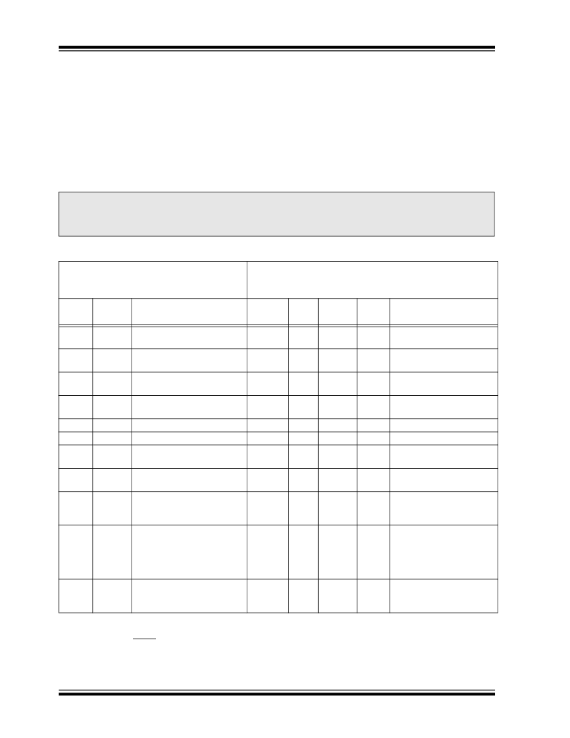
TABLE 1-1:
DC CHARACTERISTICS
NOTICE:
Stresses above those listed under “Absolute Maximum Ratings” may cause permanent damage to the
device. This is a stress rating only and functional operation of the device at those or any other conditions above those
indicated in the operational listings of this specification is not implied. Exposure to maximum rating conditions for
extended periods may affect device reliability.
All parameters apply over the specified
ranges unless otherwise noted.
V
CC
= range by device (see Table on Page 1)
Industrial (I):
T
A
= -40°C to +85°C
Automotive (E): T
A
= -40°C to +125°C
Param.
No.
Symbol
Parameter
Min
Typ
Max
Units
Conditions
D1
V
IH
1
V
IH
2
V
IL
1
V
IL
2
Vol1
Vol2
V
OH
1
V
OH
2
I
LI
I
LO
C
IN
,
C
OUT
I
CC
write Write current
High-level input voltage
2.0
0.7 V
CC
-0.3
-0.3
—
—
2.4
V
CC
- 0.2
—
—
—
—
—
—
—
—
—
—
—
—
—
—
V
CC
+1
V
CC
+1
0.8
0.2 V
CC
0.4
0.2
—
—
±1
±1
7
V
V
V
V
V
V
V
V
μ
A
μ
A
pF
V
CC
≥
2.7V
V
CC
< 2.7V
V
CC
≥
2.7V
V
CC
< 2.7V
I
OL
= 2.1 mA, V
CC
= 4.5V
I
OL
= 100
μ
A, V
CC
= 2.5V
I
OH
= -400
μ
A, V
CC
= 4.5V
I
OH
= -100
μ
A, V
CC
= 2.5V
V
IN
= V
SS
to V
CC
V
OUT
= V
SS
to V
CC
V
IN
/V
OUT
= 0V
(Note 1)
T
A
= 25°C, F
CLK
= 1 MHz
F
CLK
= 3 MHz, Vcc = 5.5V
F
CLK
= 2 MHz, Vcc = 2.5V
F
CLK
= 3 MHz, V
CC
= 5.5V
F
CLK
= 2 MHz, V
CC
= 3.0V
F
CLK
= 2 MHz, V
CC
= 2.5V
I – Temp
E – Temp
CLK = Cs = 0V
ORG = DI = V
SS
or V
CC
(Note 2) (Note 3)
D2
Low-level input voltage
D3
Low-level output voltage
D4
High-level output voltage
D5
D6
D7
Input leakage current
Output leakage current
Pin capacitance (all inputs/
outputs)
D8
—
—
—
—
—
—
—
—
500
—
—
100
—
—
2
—
1
500
—
1
5
mA
μ
A
mA
μ
A
μ
A
μ
A
μ
A
D9
I
CC
read
Read current
D10
I
CCS
Standby current
D11
V
POR
V
CC
voltage detect
93AA56A/B/C, 93LC56A/B/C
93C56A/B/C
This parameter is periodically sampled and not 100% tested.
ORG pin not available on ‘A’ or ‘B’ versions.
READY/BUSY status must be cleared from DO, see
Section 3.4 "Data Out (DO)"
.
—
—
1.5V
3.8V
—
—
V
V
(Note 1)
Note 1:
2:
3:
相關(guān)PDF資料 |
PDF描述 |
|---|---|
| 93AA56ASN | 2K Microwire Compatible Serial EEPROM |
| 93AA56AST | 2K Microwire Compatible Serial EEPROM |
| 93LC56C | 2K Microwire Compatible Serial EEPROM |
| 93LC66B | 4K 2.5V Microwire Serial EEPROM |
| 93LC66B | 4K 2.5V Microwire Serial EEPROM(4K位,2.5V,具上掉電數(shù)據(jù)保護(hù)電路,Microwire接口EEPROM) |
相關(guān)代理商/技術(shù)參數(shù) |
參數(shù)描述 |
|---|---|
| 93AA56ASN | 制造商:MICROCHIP 制造商全稱:Microchip Technology 功能描述:2K Microwire Compatible Serial EEPROM |
| 93AA56AST | 制造商:MICROCHIP 制造商全稱:Microchip Technology 功能描述:2K Microwire Compatible Serial EEPROM |
| 93AA56AT-E/CH | 制造商:MICROCHIP 制造商全稱:Microchip Technology 功能描述:1K-16K Microwire Compatible Serial EEPROMs |
| 93AA56AT-E/MC | 制造商:MICROCHIP 制造商全稱:Microchip Technology 功能描述:1K-16K Microwire Compatible Serial EEPROMs |
| 93AA56ATE/MS | 制造商:MICROCHIP 制造商全稱:Microchip Technology 功能描述:2K Microwire Compatible Serial EEPROM |
發(fā)布緊急采購,3分鐘左右您將得到回復(fù)。