- 您現(xiàn)在的位置:買賣IC網(wǎng) > PDF目錄25564 > 9DB1933AKLFT (INTEGRATED DEVICE TECHNOLOGY INC) 9DB SERIES, PLL BASED CLOCK DRIVER, 19 TRUE OUTPUT(S), 0 INVERTED OUTPUT(S), PQCC72 PDF資料下載
參數(shù)資料
| 型號(hào): | 9DB1933AKLFT |
| 廠商: | INTEGRATED DEVICE TECHNOLOGY INC |
| 元件分類: | 時(shí)鐘及定時(shí) |
| 英文描述: | 9DB SERIES, PLL BASED CLOCK DRIVER, 19 TRUE OUTPUT(S), 0 INVERTED OUTPUT(S), PQCC72 |
| 封裝: | ROHS COMPLIANT, PLASTIC, QFN-72 |
| 文件頁(yè)數(shù): | 15/17頁(yè) |
| 文件大?。?/td> | 174K |
| 代理商: | 9DB1933AKLFT |
第1頁(yè)第2頁(yè)第3頁(yè)第4頁(yè)第5頁(yè)第6頁(yè)第7頁(yè)第8頁(yè)第9頁(yè)第10頁(yè)第11頁(yè)第12頁(yè)第13頁(yè)第14頁(yè)當(dāng)前第15頁(yè)第16頁(yè)第17頁(yè)

IDT
Nineteen Output Differential Buffer for PCIe Gen3
9DB1933
Nineteen Output Differential Buffer for PCIe Gen3
7
1676A—07/12/10
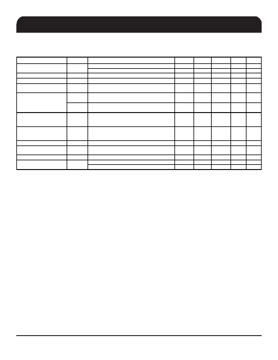
Electrical Characteristics - Output Duty Cycle, Jitter, Skew and PLL Characterisitics
TA = TCOM; Supply Voltage VDD = 3.3 V +/-5%
PARAMETER
SYMBOL
CONDITIONS
MIN
TYP
MAX
UNITS NOTES
-3dB point in High BW Mode
2
3
4
MHz
1
-3dB point in Low BW Mode
0.7
1
1.4
MHz
1
PLL Jitter Peaking
tJPEAK
Peak Pass band Gain
1.4
2
dB
1
Duty Cycle
tDC
Measured differentially, PLL Mode
45
49.5
55
%
1,2
Duty Cycle Distortion
tDCD
Measured differentially, Bypass Mode @100MHz
-2
1
2
%
1,2,5
tpdBYP
Bypass Mode, nominal value @ 25°C, 3.3V,
VT = 50%
2500
3700
4500
ps
1,2,4
tpdPLL
PLL Mode, nominal value @ 25°C, 3.3V,
VT = 50%
100
300
500
ps
1,2,3
DIF_IN, DIF [x:0]
Δtpd_BYP
Input-to-Output Skew Variation in Bypass mode
(over specified voltage / temperature operating
ranges)
|500|
|600|
ps
1,2,4,6,
7,8,9,
13
DIF_IN, DIF [x:0]
Δt
pd_PLL
Input-to-Output Skew Variation in PLL mode
(over specified voltage / temperature operating
ranges)
|250|
|350|
ps
1,2,3,6,
7,8,9,
13
DIF[X:0]
tJPH
Differential Phase Jitter (RMS Value)
2
10
ps
1,7,10
DIF[X:0]
tSSTERROR
Differential Spread Spectrum Tracking Error (peak
to peak)
40
80
ps
1,7,12
Skew, Output to Output
tsk3
VT = 50%
100
150
ps
1
PLL mode
40
50
ps1,2
Additive Jitter in Bypass Mode
25
50
ps
1,2
1Guaranteed by design and characterization, not 100% tested in production. C
LOAD = 2pF
5 Duty cycle distortion is the difference in duty cycle between the output and the input clock when the device is operated in bypass mode.
6 VT = 50% of Vout
11 t is the period of the input clock
PLL Bandwidth
BW
3 PLL mode Input-to-Output skew is measured at the first output edge following the corresponding input.
2 Measured from differential cross-point to differential cross-point
4 All Bypass Mode Input-to-Output specs refer to the timing between an input edge and the specific output edge created by it.
7 This parameter is deterministic for a given device
13 This parameter is an absolute value. It is not a double-sided figure.
Skew, Input to Output
Jitter, Cycle to cycle
9 Long-term variation from nominal of input-to-output skew over temperature and voltage for a single device.
10 This parameter is measured at the outputs of two separate 9DB1933 devices driven by a single main clock. The 9DB1933's must be
set to high bandwidth. Differential phase jitter is the accumulation of the phase jitter not shared by the outputs (eg. not including the
12 Differential spread spectrum tracking error is the difference in spread spectrum tracking between two 9DB1933 devices This parameter
is measured at the outputs of two separate 9DB1933 devices driven by a single main clock in Spread Spectrum mode. The 9DB1933's
must be set to high bandwidth. The spread spectrum characteristics are: maximum of 0.5%, 30-33KHz modulation frequency, linear
tjcyc-cyc
8 Measured with scope averaging on to find mean value.
相關(guān)PDF資料 |
PDF描述 |
|---|---|
| 9DB202CGLF | 9DB SERIES, PLL BASED CLOCK DRIVER, 2 TRUE OUTPUT(S), 0 INVERTED OUTPUT(S), PDSO20 |
| 9DB202CFLF | 9DB SERIES, PLL BASED CLOCK DRIVER, 2 TRUE OUTPUT(S), 0 INVERTED OUTPUT(S), PDSO20 |
| 9DB202CFLFT | 9DB SERIES, PLL BASED CLOCK DRIVER, 2 TRUE OUTPUT(S), 0 INVERTED OUTPUT(S), PDSO20 |
| 9DB202CK-01T | 9DB SERIES, PLL BASED CLOCK DRIVER, 1 TRUE OUTPUT(S), 0 INVERTED OUTPUT(S), QCC32 |
| 9DB206CFLF | 9DB SERIES, PLL BASED CLOCK DRIVER, 6 TRUE OUTPUT(S), 0 INVERTED OUTPUT(S), PDSO28 |
相關(guān)代理商/技術(shù)參數(shù) |
參數(shù)描述 |
|---|---|
| 9DB202CF | 制造商:Integrated Device Technology Inc 功能描述:9DB202CF - Rail/Tube |
| 9DB202CFLF | 功能描述:時(shí)鐘合成器/抖動(dòng)清除器 2 HCSL Output PCIe Buffer RoHS:否 制造商:Skyworks Solutions, Inc. 輸出端數(shù)量: 輸出電平: 最大輸出頻率: 輸入電平: 最大輸入頻率:6.1 GHz 電源電壓-最大:3.3 V 電源電壓-最小:2.7 V 封裝 / 箱體:TSSOP-28 封裝:Reel |
| 9DB202CFLFT | 功能描述:時(shí)鐘緩沖器 2 HCSL Output PCIe Buffer RoHS:否 制造商:Texas Instruments 輸出端數(shù)量:5 最大輸入頻率:40 MHz 傳播延遲(最大值): 電源電壓-最大:3.45 V 電源電壓-最小:2.375 V 最大功率耗散: 最大工作溫度:+ 85 C 最小工作溫度:- 40 C 封裝 / 箱體:LLP-24 封裝:Reel |
| 9DB202CFT | 制造商:Integrated Device Technology Inc 功能描述:9DB202CFT - Tape and Reel |
| 9DB202CG | 制造商:Integrated Device Technology Inc 功能描述:9DB202CG - Rail/Tube |
發(fā)布緊急采購(gòu),3分鐘左右您將得到回復(fù)。