- 您現(xiàn)在的位置:買賣IC網(wǎng) > PDF目錄352476 > A42MX16-1PL100I (Electronic Theatre Controls, Inc.) 40MX and 42MX FPGA Families PDF資料下載
參數(shù)資料
| 型號: | A42MX16-1PL100I |
| 廠商: | Electronic Theatre Controls, Inc. |
| 英文描述: | 40MX and 42MX FPGA Families |
| 中文描述: | 40MX和42MX FPGA系列 |
| 文件頁數(shù): | 18/120頁 |
| 文件大小: | 854K |
| 代理商: | A42MX16-1PL100I |
第1頁第2頁第3頁第4頁第5頁第6頁第7頁第8頁第9頁第10頁第11頁第12頁第13頁第14頁第15頁第16頁第17頁當(dāng)前第18頁第19頁第20頁第21頁第22頁第23頁第24頁第25頁第26頁第27頁第28頁第29頁第30頁第31頁第32頁第33頁第34頁第35頁第36頁第37頁第38頁第39頁第40頁第41頁第42頁第43頁第44頁第45頁第46頁第47頁第48頁第49頁第50頁第51頁第52頁第53頁第54頁第55頁第56頁第57頁第58頁第59頁第60頁第61頁第62頁第63頁第64頁第65頁第66頁第67頁第68頁第69頁第70頁第71頁第72頁第73頁第74頁第75頁第76頁第77頁第78頁第79頁第80頁第81頁第82頁第83頁第84頁第85頁第86頁第87頁第88頁第89頁第90頁第91頁第92頁第93頁第94頁第95頁第96頁第97頁第98頁第99頁第100頁第101頁第102頁第103頁第104頁第105頁第106頁第107頁第108頁第109頁第110頁第111頁第112頁第113頁第114頁第115頁第116頁第117頁第118頁第119頁第120頁
114
4958B–AUTO–11/10
Atmel ATA6285/ATA6286 [Preliminary]
When the SPI is enabled, the data direction of the MOSI, MISO, SCK, and pin is overridden
according Table 3-46. For more details on automatic port overrides, refer to Section 3.12.3
3.14.1
SS - Pin Functionality
3.14.1.1
Slave Mode
When the SPI is configured as a Slave, the Slave Select SS - pin is always input. When SS is
held low, the SPI is activated, and MISO becomes an output if configured by the user. All other
pins are inputs. When SS is driven high, all pins are inputs, and the SPI is passive, which means
that it will not receive incoming data. Note that the SPI logic will be reset once the SS pin is
driven high.
The SS - pin is useful for packet/byte synchronization to keep the slave bit counter synchronous
with the master clock generator. When the SS - pin is driven high, the SPI slave will immediately
reset the send and receive logic, and drop any partially received data in the Shift Register.
3.14.1.2
Master Mode
When the SPI is configured as a Master (MSTR in SPCR is set), the user can determine the
direction of the SS - pin.
If SS is configured as an output, the pin is a general output pin which does not affect the SPI
system. Typically, the pin will be driving the SS - pin of the SPI Slave.
If SS is configured as an input, it must be held high to ensure Master SPI operation. If the
SS - pin is driven low by peripheral circuitry when the SPI is configured as a Master with the
SS - pin defined as an input, the SPI system interprets this as another master, selecting the SPI
as a slave and starting to send data to it. To avoid bus contention, the SPI system takes the fol-
lowing actions:
The MSTR bit in SPCR is cleared and the SPI system becomes a Slave. As a result of the SPI
becoming a Slave, the MOSI and SCK pins become inputs.
The SPIF Flag in SPSR is set, and if the SPI interrupt is enabled, and the I-bit in SREG is set,
the interrupt routine will be executed.
Thus, when interrupt-driven SPI transmission is used in Master mode, and there exists a possi-
bility that SS is driven low, the interrupt should always check that the MSTR bit is still set. If the
MSTR bit has been cleared by a slave select, it must be set by the user to re-enable SPI Master
mode.
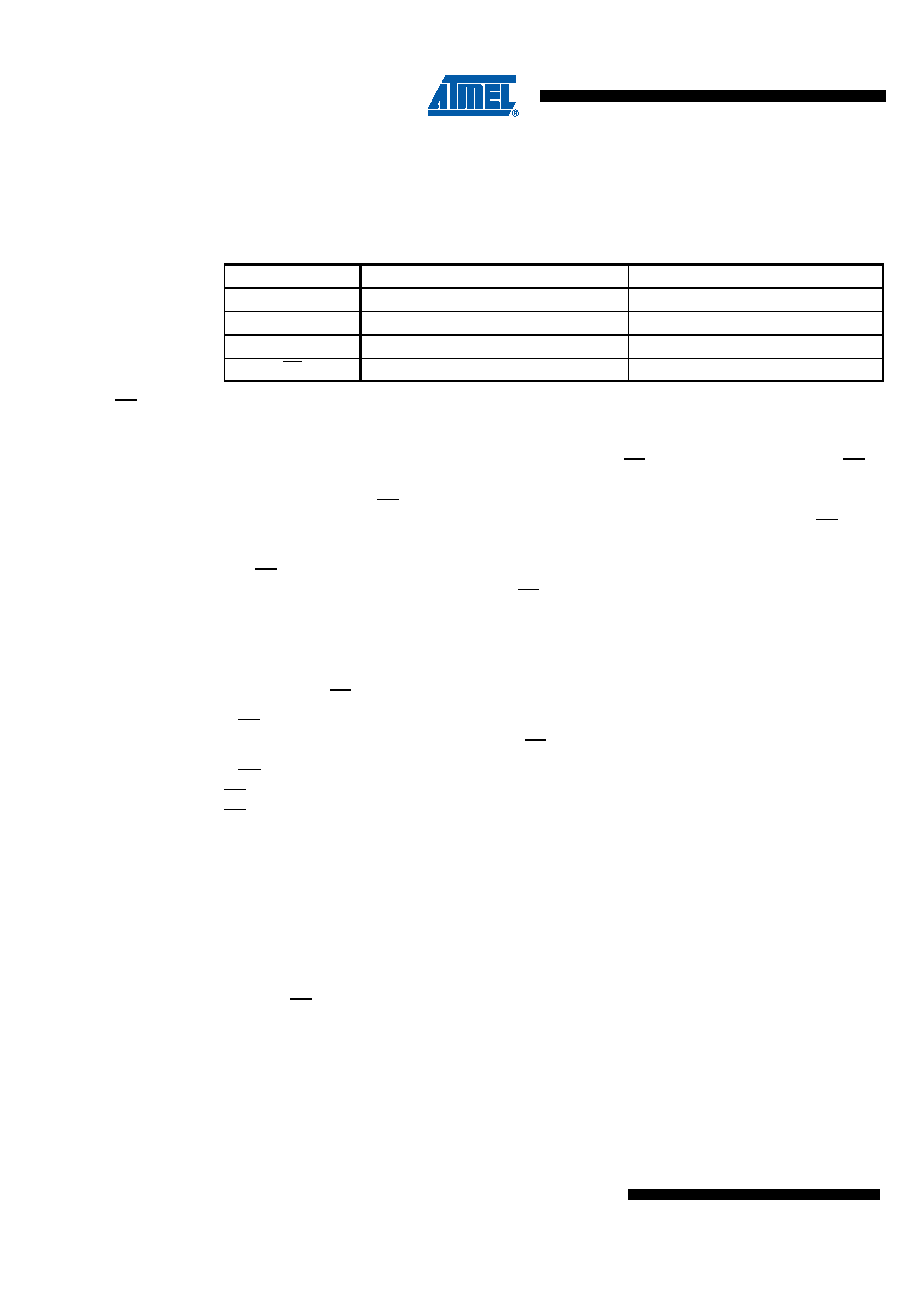
Table 3-46.
SPI Pin Overrides
Pin
Direction, Master SPI
Direction, Slave SPI
MOSI
User Defined
Input
MISO
Input
User Defined
SCK
User Defined
Input
SS
User Defined
Input
相關(guān)PDF資料 |
PDF描述 |
|---|---|
| A42MX16-1PL100M | IC TVS BI-DIR 24V 350W SOD-323 |
| A42MX02-1BG100 | 40MX and 42MX FPGA Families |
| A42MX04-1BG100 | 40MX and 42MX FPGA Families |
| A42MX09-1BG100 | 40MX and 42MX FPGA Families |
| A42MX24-1BG100 | 40MX and 42MX FPGA Families |
相關(guān)代理商/技術(shù)參數(shù) |
參數(shù)描述 |
|---|---|
| A42MX16-1PL100M | 制造商:ACTEL 制造商全稱:Actel Corporation 功能描述:40MX and 42MX FPGA Families |
| A42MX16-1PL84 | 功能描述:IC FPGA MX SGL CHIP 24K 84-PLCC RoHS:否 類別:集成電路 (IC) >> 嵌入式 - FPGA(現(xiàn)場可編程門陣列) 系列:MX 標(biāo)準(zhǔn)包裝:40 系列:SX-A LAB/CLB數(shù):6036 邏輯元件/單元數(shù):- RAM 位總計(jì):- 輸入/輸出數(shù):360 門數(shù):108000 電源電壓:2.25 V ~ 5.25 V 安裝類型:表面貼裝 工作溫度:0°C ~ 70°C 封裝/外殼:484-BGA 供應(yīng)商設(shè)備封裝:484-FPBGA(27X27) |
| A42MX16-1PL84I | 功能描述:IC FPGA MX SGL CHIP 24K 84-PLCC RoHS:否 類別:集成電路 (IC) >> 嵌入式 - FPGA(現(xiàn)場可編程門陣列) 系列:MX 標(biāo)準(zhǔn)包裝:40 系列:SX-A LAB/CLB數(shù):6036 邏輯元件/單元數(shù):- RAM 位總計(jì):- 輸入/輸出數(shù):360 門數(shù):108000 電源電壓:2.25 V ~ 5.25 V 安裝類型:表面貼裝 工作溫度:0°C ~ 70°C 封裝/外殼:484-BGA 供應(yīng)商設(shè)備封裝:484-FPBGA(27X27) |
| A42MX16-1PL84M | 制造商:Microsemi Corporation 功能描述:FPGA 42MX Family 24K Gates 608 Cells 119MHz/198MHz 0.45um Technology 3.3V/5V 84-Pin PLCC 制造商:Microsemi Corporation 功能描述:FPGA 24K GATES 608 CELLS 119MHZ/198MHZ 0.45UM 3.3V/5V 84PLCC - Rail/Tube 制造商:Microsemi Corporation 功能描述:IC FPGA 72 I/O 84PLCC 制造商:Microsemi Corporation 功能描述:IC FPGA MX SGL CHIP 24K 84-PLCC |
| A42MX16-1PLG84 | 功能描述:IC FPGA MX SGL CHIP 24K 84-PLCC RoHS:是 類別:集成電路 (IC) >> 嵌入式 - FPGA(現(xiàn)場可編程門陣列) 系列:MX 標(biāo)準(zhǔn)包裝:40 系列:SX-A LAB/CLB數(shù):6036 邏輯元件/單元數(shù):- RAM 位總計(jì):- 輸入/輸出數(shù):360 門數(shù):108000 電源電壓:2.25 V ~ 5.25 V 安裝類型:表面貼裝 工作溫度:0°C ~ 70°C 封裝/外殼:484-BGA 供應(yīng)商設(shè)備封裝:484-FPBGA(27X27) |
發(fā)布緊急采購,3分鐘左右您將得到回復(fù)。