- 您現在的位置:買賣IC網 > PDF目錄362029 > A54SX08-1PL84M Field Programmable Gate Array (FPGA) PDF資料下載
參數資料
| 型號: | A54SX08-1PL84M |
| 英文描述: | Field Programmable Gate Array (FPGA) |
| 中文描述: | 現場可編程門陣列(FPGA) |
| 文件頁數: | 11/36頁 |
| 文件大小: | 833K |
| 代理商: | A54SX08-1PL84M |
第1頁第2頁第3頁第4頁第5頁第6頁第7頁第8頁第9頁第10頁當前第11頁第12頁第13頁第14頁第15頁第16頁第17頁第18頁第19頁第20頁第21頁第22頁第23頁第24頁第25頁第26頁第27頁第28頁第29頁第30頁第31頁第32頁第33頁第34頁第35頁第36頁
v2.0
11
54SX Family FPGAs RadTolerant and HiRel
3.3V/5V Operating Conditions
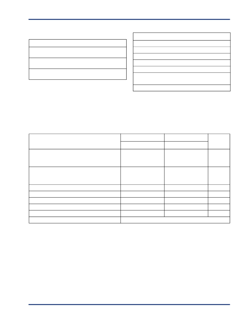
Recommended Operating Conditions
1
Parameter
Commercial
Military
Units
Temperature
Range
1
3.3V Power
2
Supply Tolerance
5V Power Supply
2
Tolerance
0 to +70
–
55 to +125
°
C
±
10
±
10
%V
CC
±
5
±
10
%V
CC
Notes:
1.
Ambient temperature (T
A
) is used for commercial and
industrial; case temperature (T
C
) is used for military.
All power supplies must be in the recommended operating range
for 250μs. For more information, please refer to the
Power-Up
Design
Considerations
http://www.actel.com/appnotes
.
2.
application
note
at
Recommended Operating Conditions
Symbol
Parameter
Limits
Units
V
CCR
V
CCA
V
CCI
V
I
V
O
DC Supply Voltage
–
0.3 to +6.0
V
DC Supply Voltage
–
0.3 to +4.0
V
DC Supply Voltage
–
0.3 to +4.0
V
Input Voltage
–
0.5 to +5.5
V
Output Voltage
–
0.5 to +3.6
V
I
IO
I/O Source Sink
Current
2
–
30 to +5.0
mA
T
STG
Notes:
1.
Storage Temperature
–
40 to +125
°
C
Stresses beyond those listed in the Absolute Maximum Ratings
table may cause permanent damage to the device. Exposure to
absolute maximum rated conditions for extended periods may
affect device reliability. Device should not be operated outside
the Recommended Operating Conditions.
The I/O source sink numbers refer to tristated inputs and
outputs
2.
Electrical Specifications
Commercial
Military
Symbol
Parameter
Min.
Max.
Min.
Max.
Units
V
OH
(I
OH
=
–
20μA) (CMOS)
(I
OH
=
–
8mA) (TTL)
(I
OH
=
–
6mA) (TTL)
(I
OL
= 20μA) (CMOS)
(I
OL
= 12mA) (TTL)
(I
OL
= 8mA) (TTL)
Low Level Inputs
(V
CCI
–
0.1)
2.4
V
CCI
V
CCI
(V
CCI
–
0.1)
2.4
V
CCI
V
CCI
V
V
OL
0.10
0.50
0.50
V
V
IL
V
IH
t
R
, t
F
C
IO
I
CC
I
CC(D)
0.8
0.8
V
High Level Inputs
2.0
2.0
V
Input Transition Time t
R
, t
F
C
IO
I/O Capacitance
Standby Current, I
CC
I
CC(D)
I
Dynamic
V
CC
Supply Current
50
50
ns
10
10
pF
4.0
25
mA
See the
“
Power Dissipation
”
section on page 13.
相關PDF資料 |
PDF描述 |
|---|---|
| A54SX08-1TQ144 | Field Programmable Gate Array (FPGA) |
| A54SX08-1TQ144I | Field Programmable Gate Array (FPGA) |
| A54SX08-1TQ144M | Field Programmable Gate Array (FPGA) |
| A54SX08-1TQ176 | Field Programmable Gate Array (FPGA) |
| A54SX08-1TQ176I | Field Programmable Gate Array (FPGA) |
相關代理商/技術參數 |
參數描述 |
|---|---|
| A54SX08-1PLG84 | 功能描述:IC FPGA SX 12K GATES 84-PLCC RoHS:是 類別:集成電路 (IC) >> 嵌入式 - FPGA(現場可編程門陣列) 系列:SX 標準包裝:40 系列:SX-A LAB/CLB數:6036 邏輯元件/單元數:- RAM 位總計:- 輸入/輸出數:360 門數:108000 電源電壓:2.25 V ~ 5.25 V 安裝類型:表面貼裝 工作溫度:0°C ~ 70°C 封裝/外殼:484-BGA 供應商設備封裝:484-FPBGA(27X27) |
| A54SX08-1PLG84I | 功能描述:IC FPGA SX 12K GATES 84-PLCC RoHS:是 類別:集成電路 (IC) >> 嵌入式 - FPGA(現場可編程門陣列) 系列:SX 標準包裝:40 系列:SX-A LAB/CLB數:6036 邏輯元件/單元數:- RAM 位總計:- 輸入/輸出數:360 門數:108000 電源電壓:2.25 V ~ 5.25 V 安裝類型:表面貼裝 工作溫度:0°C ~ 70°C 封裝/外殼:484-BGA 供應商設備封裝:484-FPBGA(27X27) |
| A54SX08-1PQ208 | 功能描述:IC FPGA SX 12K GATES 208-PQFP RoHS:否 類別:集成電路 (IC) >> 嵌入式 - FPGA(現場可編程門陣列) 系列:SX 標準包裝:40 系列:SX-A LAB/CLB數:6036 邏輯元件/單元數:- RAM 位總計:- 輸入/輸出數:360 門數:108000 電源電壓:2.25 V ~ 5.25 V 安裝類型:表面貼裝 工作溫度:0°C ~ 70°C 封裝/外殼:484-BGA 供應商設備封裝:484-FPBGA(27X27) |
| A54SX08-1PQ208I | 功能描述:IC FPGA SX 12K GATES 208-PQFP RoHS:否 類別:集成電路 (IC) >> 嵌入式 - FPGA(現場可編程門陣列) 系列:SX 標準包裝:40 系列:SX-A LAB/CLB數:6036 邏輯元件/單元數:- RAM 位總計:- 輸入/輸出數:360 門數:108000 電源電壓:2.25 V ~ 5.25 V 安裝類型:表面貼裝 工作溫度:0°C ~ 70°C 封裝/外殼:484-BGA 供應商設備封裝:484-FPBGA(27X27) |
| A54SX08-1PQ208M | 制造商:未知廠家 制造商全稱:未知廠家 功能描述:54SX Family FPGAs |
發(fā)布緊急采購,3分鐘左右您將得到回復。