- 您現(xiàn)在的位置:買賣IC網(wǎng) > PDF目錄362029 > A54SX32-2BG313 Field Programmable Gate Array (FPGA) PDF資料下載
參數(shù)資料
| 型號: | A54SX32-2BG313 |
| 英文描述: | Field Programmable Gate Array (FPGA) |
| 中文描述: | 現(xiàn)場可編程門陣列(FPGA) |
| 文件頁數(shù): | 24/36頁 |
| 文件大?。?/td> | 833K |
| 代理商: | A54SX32-2BG313 |
第1頁第2頁第3頁第4頁第5頁第6頁第7頁第8頁第9頁第10頁第11頁第12頁第13頁第14頁第15頁第16頁第17頁第18頁第19頁第20頁第21頁第22頁第23頁當(dāng)前第24頁第25頁第26頁第27頁第28頁第29頁第30頁第31頁第32頁第33頁第34頁第35頁第36頁
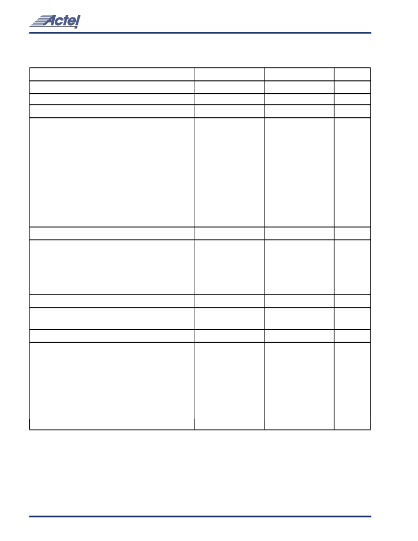
54SX Family FPGAs RadTolerant and HiRel
24
v2.0
RT54SX32 Timing Characteristics
(Worst-Case Military Conditions, V
CCR
= 4.75V, V
CCA,
V
CCI
= 3.0V, T
J
= 125
°
C)
C-Cell Propagation Delays
1
‘–
1
’
Speed
‘
Std
’
Speed
Parameter
Description
Min.
Max.
Min.
Max.
Units
t
PD
Predicted Routing Delays
2
Internal Array Module
1.7
1.8
ns
t
DC
t
FC
t
RD1
t
RD2
t
RD3
t
RD4
t
RD8
t
RD12
t
RD18
t
RD24
FO=1 Routing Delay, Direct Connect
0.2
0.2
ns
FO=1 Routing Delay, Fast Connect
1.1
1.3
ns
FO=1 Routing Delay
1.3
1.5
ns
FO=2 Routing Delay
2.2
2.6
ns
FO=3 Routing Delay
3.1
3.6
ns
FO=4 Routing Delay
4.0
4.7
ns
FO=8 Routing Delay
7.8
9.0
ns
FO=12 Routing Delay
10.1
11.9
ns
FO=18 Routing Delay
17.0
19.8
ns
FO=24 Routing Delay
22.4
26.3
ns
R-Cell Timing
t
RCO
t
CLR
t
SUD
t
HD
t
WASYN
Sequential Clock-to-Q
1.5
2.0
ns
Asynchronous Clear-to-Q
1.5
2.0
ns
Flip-Flop Data Input Set-Up
2.0
2.2
ns
Flip-Flop Data Input Hold
0.0
0.0
ns
Asynchronous Pulse Width
4.4
5.3
ns
I/O Module Input Propagation Delays
t
INYH
t
INYL
Predicted Input Routing Delays
3
Input Data Pad-to-Y HIGH
4.0
4.7
ns
Input Data Pad-to-Y LOW
4.0
4.7
ns
t
IRD1
t
IRD2
t
IRD3
t
IRD4
t
IRD8
t
IRD12
t
IRD18
t
IRD24
Notes:
1.
2.
FO=1 Routing Delay
1.3
1.5
ns
FO=2 Routing Delay
2.2
2.6
ns
FO=3 Routing Delay
3.1
3.6
ns
FO=4 Routing Delay
4.0
4.7
ns
FO=8 Routing Delay
7.8
9.0
ns
FO=12 Routing Delay
10.1
11.9
ns
FO=18 Routing Delay
17.0
19.8
ns
FO=24 Routing Delay
22.4
26.3
ns
For dual-module macros, use t
PD
+ t
RD1
+ t
PDn
, t
RCO
+ t
RD1
+ t
PDn
or t
PD1
+ t
RD1
+ t
SUD
, whichever is appropriate.
Routing delays are for typical designs across worst-case operating conditions. These parameters should be used for estimating device
performance. Post-route timing analysis or simulation is required to determine actual worst-case performance. Post-route timing is
based on actual routing delay measurements performed on the device prior to shipment.
3.
相關(guān)PDF資料 |
PDF描述 |
|---|---|
| A54SX32-2BG313I | Field Programmable Gate Array (FPGA) |
| A54SX32-2BG329 | Field Programmable Gate Array (FPGA) |
| A54SX32-2BG329I | Field Programmable Gate Array (FPGA) |
| A54SX32-2TQ144 | Field Programmable Gate Array (FPGA) |
| A54SX32-2TQ144I | Field Programmable Gate Array (FPGA) |
相關(guān)代理商/技術(shù)參數(shù) |
參數(shù)描述 |
|---|---|
| A54SX32-2BG313I | 功能描述:IC FPGA SX 48K GATES 313-BGA RoHS:否 類別:集成電路 (IC) >> 嵌入式 - FPGA(現(xiàn)場可編程門陣列) 系列:SX 產(chǎn)品培訓(xùn)模塊:Three Reasons to Use FPGA's in Industrial Designs Cyclone IV FPGA Family Overview 特色產(chǎn)品:Cyclone? IV FPGAs 標(biāo)準(zhǔn)包裝:60 系列:CYCLONE® IV GX LAB/CLB數(shù):9360 邏輯元件/單元數(shù):149760 RAM 位總計:6635520 輸入/輸出數(shù):270 門數(shù):- 電源電壓:1.16 V ~ 1.24 V 安裝類型:表面貼裝 工作溫度:0°C ~ 85°C 封裝/外殼:484-BGA 供應(yīng)商設(shè)備封裝:484-FBGA(23x23) |
| A54SX32-2BG329 | 功能描述:IC FPGA SX 48K GATES 329-BGA RoHS:否 類別:集成電路 (IC) >> 嵌入式 - FPGA(現(xiàn)場可編程門陣列) 系列:SX 產(chǎn)品培訓(xùn)模塊:Three Reasons to Use FPGA's in Industrial Designs Cyclone IV FPGA Family Overview 特色產(chǎn)品:Cyclone? IV FPGAs 標(biāo)準(zhǔn)包裝:60 系列:CYCLONE® IV GX LAB/CLB數(shù):9360 邏輯元件/單元數(shù):149760 RAM 位總計:6635520 輸入/輸出數(shù):270 門數(shù):- 電源電壓:1.16 V ~ 1.24 V 安裝類型:表面貼裝 工作溫度:0°C ~ 85°C 封裝/外殼:484-BGA 供應(yīng)商設(shè)備封裝:484-FBGA(23x23) |
| A54SX32-2BG329I | 功能描述:IC FPGA SX 48K GATES 329-BGA RoHS:否 類別:集成電路 (IC) >> 嵌入式 - FPGA(現(xiàn)場可編程門陣列) 系列:SX 產(chǎn)品培訓(xùn)模塊:Three Reasons to Use FPGA's in Industrial Designs Cyclone IV FPGA Family Overview 特色產(chǎn)品:Cyclone? IV FPGAs 標(biāo)準(zhǔn)包裝:60 系列:CYCLONE® IV GX LAB/CLB數(shù):9360 邏輯元件/單元數(shù):149760 RAM 位總計:6635520 輸入/輸出數(shù):270 門數(shù):- 電源電壓:1.16 V ~ 1.24 V 安裝類型:表面貼裝 工作溫度:0°C ~ 85°C 封裝/外殼:484-BGA 供應(yīng)商設(shè)備封裝:484-FBGA(23x23) |
| A54SX32-2BG329IX3 | 制造商:Microsemi Corporation 功能描述:FPGA SX Family 32K Gates 1800 Cells 320MHz 0.35um Technology 3.3V/5V 329-Pin BGA 制造商:Microsemi Corporation 功能描述:54SX 32K GATES 1800 MC 320MHZ IND CMOS 3.3/5V 329 BGA - Trays |
| A54SX32-2BGG329 | 功能描述:IC FPGA SX 48K GATES 329-BGA RoHS:是 類別:集成電路 (IC) >> 嵌入式 - FPGA(現(xiàn)場可編程門陣列) 系列:SX 產(chǎn)品培訓(xùn)模塊:Three Reasons to Use FPGA's in Industrial Designs Cyclone IV FPGA Family Overview 特色產(chǎn)品:Cyclone? IV FPGAs 標(biāo)準(zhǔn)包裝:60 系列:CYCLONE® IV GX LAB/CLB數(shù):9360 邏輯元件/單元數(shù):149760 RAM 位總計:6635520 輸入/輸出數(shù):270 門數(shù):- 電源電壓:1.16 V ~ 1.24 V 安裝類型:表面貼裝 工作溫度:0°C ~ 85°C 封裝/外殼:484-BGA 供應(yīng)商設(shè)備封裝:484-FBGA(23x23) |
發(fā)布緊急采購,3分鐘左右您將得到回復(fù)。