- 您現(xiàn)在的位置:買賣IC網(wǎng) > PDF目錄362029 > A54SX32-2BG313 Field Programmable Gate Array (FPGA) PDF資料下載
參數(shù)資料
| 型號: | A54SX32-2BG313 |
| 英文描述: | Field Programmable Gate Array (FPGA) |
| 中文描述: | 現(xiàn)場可編程門陣列(FPGA) |
| 文件頁數(shù): | 5/36頁 |
| 文件大?。?/td> | 833K |
| 代理商: | A54SX32-2BG313 |
第1頁第2頁第3頁第4頁當前第5頁第6頁第7頁第8頁第9頁第10頁第11頁第12頁第13頁第14頁第15頁第16頁第17頁第18頁第19頁第20頁第21頁第22頁第23頁第24頁第25頁第26頁第27頁第28頁第29頁第30頁第31頁第32頁第33頁第34頁第35頁第36頁
v2.0
5
54SX Family FPGAs RadTolerant and HiRel
architecture. An example of the improved flexibility
enabled by the inversion capability is the ability to integrate
a 3-input exclusive-OR function into a single C-cell. This
facilitates construction of 9-bit parity-tree functions with 2
ns propagation delays. At the same time, the C-cell
structure is extremely synthesis-friendly, simplifying the
overall design and reducing synthesis time.
Chip Architecture
The
SX
uniqueapproach to module organization and chip routing
that delivers the best register/logic mix for a wide variety of
new and emerging applications.
family
’
s
chip
architecture
provides
a
Module Organization
Actel has arranged all C-cell and R-cell logic modules into
horizontal banks called
Clusters
. There are two types of
Clusters: Type 1 contains two C-cells and one R-cell, while
Type 2 contains one C-cell and two R-cells.
To increase design efficiency and device performance, Actel
has further organized these modules into
SuperClusters
(see
Figure 5 on page 6
). SuperCluster 1 is a two-wide
grouping of Type 1 clusters. SuperCluster 2 is a two-wide
group containing one Type 1 cluster and one Type 2 cluster.
SX devices feature more SuperCluster 1 modules than
SuperCluster 2 modules because designers typically require
more combinatorial logic than flip-flops.
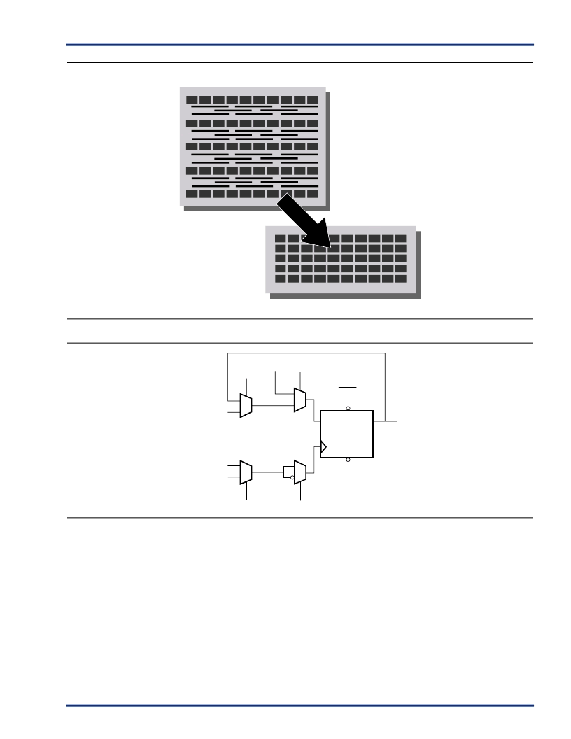
Figure 2
Channelled Array and Sea-of-Modules Architectures
Figure 3
R-Cell
Channelled Array Architecture
Sea-of-Modules Architecture
Direct
Connect
Input
CLKA,
CLKB
HCLK
CKS
CKP
CLRB
PSET
Y
D
Q
Routed
Data Input
S0
S1
相關PDF資料 |
PDF描述 |
|---|---|
| A54SX32-2BG313I | Field Programmable Gate Array (FPGA) |
| A54SX32-2BG329 | Field Programmable Gate Array (FPGA) |
| A54SX32-2BG329I | Field Programmable Gate Array (FPGA) |
| A54SX32-2TQ144 | Field Programmable Gate Array (FPGA) |
| A54SX32-2TQ144I | Field Programmable Gate Array (FPGA) |
相關代理商/技術參數(shù) |
參數(shù)描述 |
|---|---|
| A54SX32-2BG313I | 功能描述:IC FPGA SX 48K GATES 313-BGA RoHS:否 類別:集成電路 (IC) >> 嵌入式 - FPGA(現(xiàn)場可編程門陣列) 系列:SX 產品培訓模塊:Three Reasons to Use FPGA's in Industrial Designs Cyclone IV FPGA Family Overview 特色產品:Cyclone? IV FPGAs 標準包裝:60 系列:CYCLONE® IV GX LAB/CLB數(shù):9360 邏輯元件/單元數(shù):149760 RAM 位總計:6635520 輸入/輸出數(shù):270 門數(shù):- 電源電壓:1.16 V ~ 1.24 V 安裝類型:表面貼裝 工作溫度:0°C ~ 85°C 封裝/外殼:484-BGA 供應商設備封裝:484-FBGA(23x23) |
| A54SX32-2BG329 | 功能描述:IC FPGA SX 48K GATES 329-BGA RoHS:否 類別:集成電路 (IC) >> 嵌入式 - FPGA(現(xiàn)場可編程門陣列) 系列:SX 產品培訓模塊:Three Reasons to Use FPGA's in Industrial Designs Cyclone IV FPGA Family Overview 特色產品:Cyclone? IV FPGAs 標準包裝:60 系列:CYCLONE® IV GX LAB/CLB數(shù):9360 邏輯元件/單元數(shù):149760 RAM 位總計:6635520 輸入/輸出數(shù):270 門數(shù):- 電源電壓:1.16 V ~ 1.24 V 安裝類型:表面貼裝 工作溫度:0°C ~ 85°C 封裝/外殼:484-BGA 供應商設備封裝:484-FBGA(23x23) |
| A54SX32-2BG329I | 功能描述:IC FPGA SX 48K GATES 329-BGA RoHS:否 類別:集成電路 (IC) >> 嵌入式 - FPGA(現(xiàn)場可編程門陣列) 系列:SX 產品培訓模塊:Three Reasons to Use FPGA's in Industrial Designs Cyclone IV FPGA Family Overview 特色產品:Cyclone? IV FPGAs 標準包裝:60 系列:CYCLONE® IV GX LAB/CLB數(shù):9360 邏輯元件/單元數(shù):149760 RAM 位總計:6635520 輸入/輸出數(shù):270 門數(shù):- 電源電壓:1.16 V ~ 1.24 V 安裝類型:表面貼裝 工作溫度:0°C ~ 85°C 封裝/外殼:484-BGA 供應商設備封裝:484-FBGA(23x23) |
| A54SX32-2BG329IX3 | 制造商:Microsemi Corporation 功能描述:FPGA SX Family 32K Gates 1800 Cells 320MHz 0.35um Technology 3.3V/5V 329-Pin BGA 制造商:Microsemi Corporation 功能描述:54SX 32K GATES 1800 MC 320MHZ IND CMOS 3.3/5V 329 BGA - Trays |
| A54SX32-2BGG329 | 功能描述:IC FPGA SX 48K GATES 329-BGA RoHS:是 類別:集成電路 (IC) >> 嵌入式 - FPGA(現(xiàn)場可編程門陣列) 系列:SX 產品培訓模塊:Three Reasons to Use FPGA's in Industrial Designs Cyclone IV FPGA Family Overview 特色產品:Cyclone? IV FPGAs 標準包裝:60 系列:CYCLONE® IV GX LAB/CLB數(shù):9360 邏輯元件/單元數(shù):149760 RAM 位總計:6635520 輸入/輸出數(shù):270 門數(shù):- 電源電壓:1.16 V ~ 1.24 V 安裝類型:表面貼裝 工作溫度:0°C ~ 85°C 封裝/外殼:484-BGA 供應商設備封裝:484-FBGA(23x23) |
發(fā)布緊急采購,3分鐘左右您將得到回復。