- 您現(xiàn)在的位置:買賣IC網(wǎng) > PDF目錄362044 > AB-100 AB-100 - MULTIPLEXER DATA ACQUISTION SYSTEM PDF資料下載
參數(shù)資料
| 型號(hào): | AB-100 |
| 英文描述: | AB-100 - MULTIPLEXER DATA ACQUISTION SYSTEM |
| 中文描述: | 抗體- 100 -多路轉(zhuǎn)換數(shù)據(jù)采集系統(tǒng) |
| 文件頁數(shù): | 1/6頁 |
| 文件大小: | 69K |
| 代理商: | AB-100 |
Mailing Address: PO Box 11400 Tucson, AZ 85734 Street Address: 6730 S. Tucson Blvd. Tucson, AZ 85706
Tel: (520) 746-1111 Twx: 910-952-111 Telex: 066-6491 FAX (520) 889-1510 Immediate Product Info: (800) 548-6132
MULTIPLEXER DATA ACQUISTION SYSTEM
By Juergen Metzger, Burr-Brown International, Gmbh
1995 Burr-Brown Corporation
AB-100
Printed in U.S.A. October, 1995
The information provided herein is believed to be reliable; however, BURR-BROWN assumes
no responsibility for inaccuracies or omissions. BURR-BROWN assumes no responsibility for
the use of this information, and all use of such information shall be entirely at the user’s own
risk. Prices and specifications are subject to change without notice. No patent rights or licenses
to any of the circuits described herein are implied or granted to any third party. BURR-BROWN
does not authorize or warrant any BURR-BROWN product for use in life support devices and/
or systems.
MULTIPLEXERS GENERATE STEEP SIGNAL
EDGES AND TRANSPORT THE CHARGE
Multiplexers have been used for acquisition of quasi-static
signals for a long time. While these signals usually have a
low bandwidth of only a few hertz, applications generally
require that the multiplexer send each signal as fast as
possible to the converter and that the signals be processed
quickly. To ensure fast processing, such acquisition systems
usually include a sense amplifier behind the multiplexer to
adjust the signal level to the analog-to-digital converter and
to prevent current caused by the signals coming from the
multiplexer. But as common as this configuration is today,
it still produces unexpected errors again and again.
Unless the multiplexer is driven in low-impedance mode or
from a capacitive source, charge transmission from one
channel to another can be expected. Errors the size of several
LSBs of a 12-bit converter can arise, especially in passive
low-pass circuits in front of the input, such as those used for
EMC rejection, ESD, and overvoltage protection.
Besides leakage currents, which are very small in modern
designs, important factors are the switching of the multi-
plexer output capacitance and of the input current from the
succeeding sense amplifiers, which are usually dynamically
overloaded at the time of switching.
DYNAMIC OVERLOAD
Multiplexers switch from one channel to the next in a few
nanoseconds. This switching produces a correspondingly
steep signal pulse for the succeeding sense amplifier. This
steep edge, however, is only compensated by feedback
amplifiers after the settling time has finished. Using the
example of an op amp, this process is easy to explain.
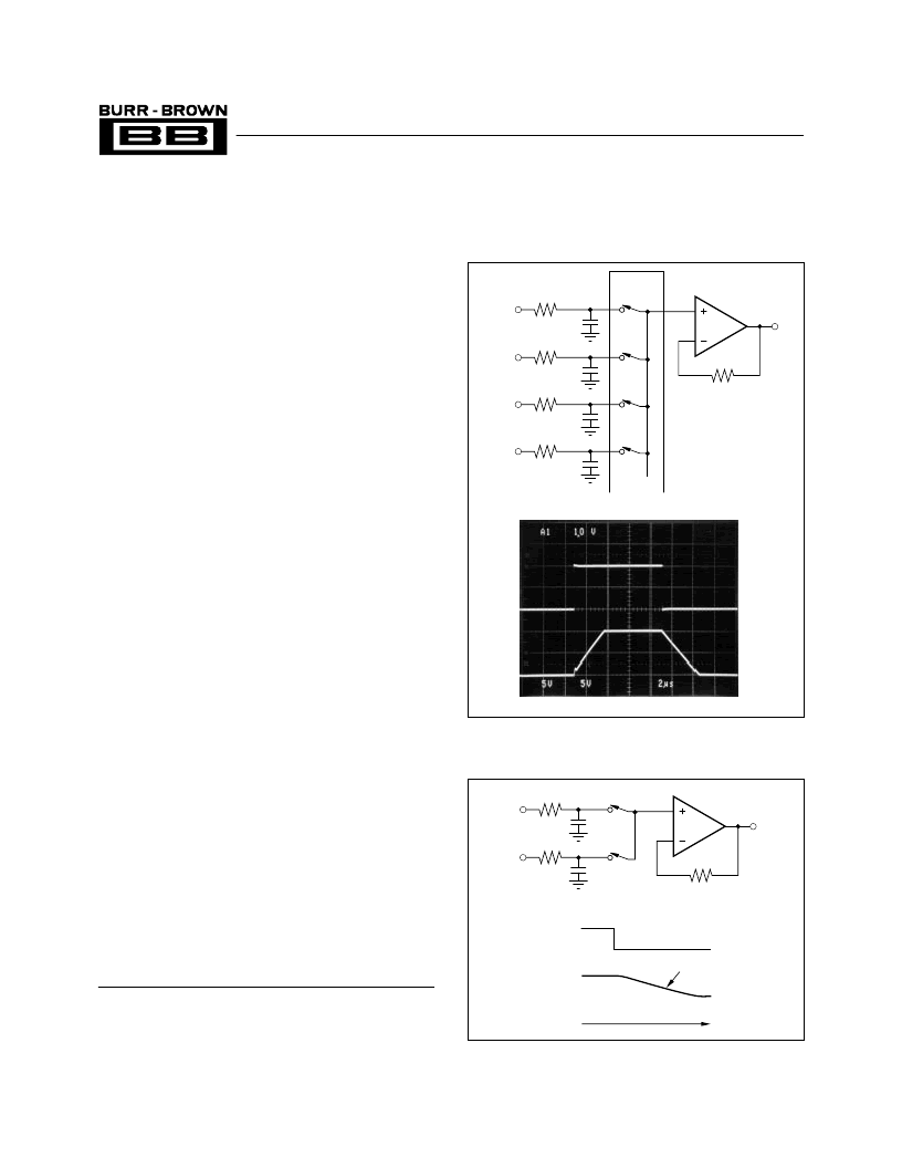
Settling time with an op amp: there is +10V at channel 1 and
0V at channel 2 (see Figure 2). The switching produces a
voltage step from 10V to 0V. The output of the op amp also
goes from 10V to 0V in a few microseconds, depending
upon the slew rate. Meanwhile, a stress flow arises at the
input with a peak value of 10V since the feedback input of
the op amp is connected to the output.
10k
MUX
10k
100nF
10V
10k
100nF
0V
10k
100nF
10k
100nF
t
V
OUT
V
IN
Slew Rate
10k
10k
100nF
10V
10k
100nF
0V
V
OUT
V
IN
FIGURE 2. Overload of the Op Amp Caused by Fast
Switching.
FIGURE 1. Step Response of Single-Ended Multiplexer,
Switching Between 0V and +10V.
相關(guān)PDF資料 |
PDF描述 |
|---|---|
| AB-101 | AB-101 - COMBINING AN AMPLIFIER WITH THE BUF634 |
| AB-102 | AB-102 - OUTPUT SPECTRUM AND POST-LPF DESIGN OF THE PCM1710 |
| AB-103 | AB-103 - NOISE ANALYSIS FOR HIGH SPEED OP AMPS |
| AB-104 | |
| AB-105 | AB-105 - TUNING IN AMPLIFIERS |
相關(guān)代理商/技術(shù)參數(shù) |
參數(shù)描述 |
|---|---|
| AB100 1/2 | 制造商:Thomas & Betts 功能描述:(SPRINGLESS NUT - EG) |
| AB100 1/2SS | 制造商:Thomas & Betts 功能描述:(6SS SPRINGLESS NUT) |
| AB100 1/4 | 制造商:Thomas & Betts 功能描述:(SPRINGLESS NUT - EG) |
| AB100 1/4SS | 制造商:Thomas & Betts 功能描述:(6SS SPRINGLESS NUT) |
| AB100 3/4 | 制造商:Thomas & Betts 功能描述:(SPRINGLESS NUT) |
發(fā)布緊急采購(gòu),3分鐘左右您將得到回復(fù)。