- 您現(xiàn)在的位置:買賣IC網(wǎng) > PDF目錄362098 > AD662BQ 12-Bit Digital-to-Analog Converter PDF資料下載
參數(shù)資料
| 型號: | AD662BQ |
| 英文描述: | 12-Bit Digital-to-Analog Converter |
| 中文描述: | 12位數(shù)字到模擬轉(zhuǎn)換器 |
| 文件頁數(shù): | 4/40頁 |
| 文件大小: | 927K |
| 代理商: | AD662BQ |
第1頁第2頁第3頁當(dāng)前第4頁第5頁第6頁第7頁第8頁第9頁第10頁第11頁第12頁第13頁第14頁第15頁第16頁第17頁第18頁第19頁第20頁第21頁第22頁第23頁第24頁第25頁第26頁第27頁第28頁第29頁第30頁第31頁第32頁第33頁第34頁第35頁第36頁第37頁第38頁第39頁第40頁
REV. A
–4–
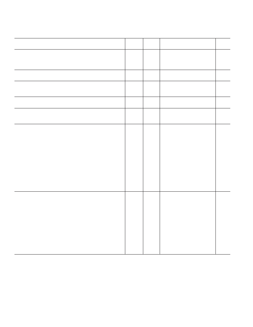
AD6624–SPECIFICATIONS
GENERAL TIMING CHARACTERISTICS
1, 2
Test
Level
AD6624AS
Typ
Parameter (Conditions)
Temp
Min
Max
Unit
CLK Timing Requirements
:
t
CLK
CLK Period
t
CLKL
CLK Width Low
t
CLKH
CLK Width High
RESET
Timing Requirement
:
t
RESL
RESET
Width Low
Input Wideband Data Timing Requirements
:
t
SI
Input to
↑
CLK Setup Time
t
HI
Input to
↑
CLK Hold Time
Level Indicator Output Switching Characteristic
:
t
DLI
↑
CLK to LI (A–A, B; B–A, B) Output Delay Time
SYNC Timing Requirements
:
t
SS
SYNC (A, B, C, D) to
↑
CLK Setup Time
t
HS
SYNC (A, B, C, D) to
↑
CLK Hold Time
Serial Port Timing Requirements
(
SBM = 1
):
Switching Characteristics
:
3
t
DSCLK1
↑
CLK to
↑
SCLK Delay (Divide by 1)
t
DSCLKH
↑
CLK to
↑
SCLK Delay (For Any Other Divisor)
t
DSCLKL
↑
CLK to
↓
SCLK Delay (Divide by 2 or Even #)
t
DSCLKLL
↓
CLK to
↓
SCLK Delay (Divide by 3 or Odd #)
t
DSDFS
↑
SCLK to SDFS Delay
t
DSDFE
↑
SCLK to SDFE Delay
t
DSDO
↑
SCLK to SDO Delay
t
DSDR
↑
SCLK to DR Delay
t
DDR
↑
CLK to DR Delay
Input Characteristics
:
t
SSI
SDI to
↓
SCLK Setup Time
t
HSI
SDI to
↓
SCLK Hold Time
Serial Port Timing Requirements
(
SBM = 0
):
Switching Characteristics
:
3
t
SCLK
SCLK Period
t
SCLKL
SCLK Low Time (When SDIV = 1, Divide by 1)
t
SCLKH
SCLK High Time (When SDIV = 1, Divide by 1)
t
DSDFE
↑
SCLK to SDFE Delay
t
DSDO
↑
SCLK to SDO Delay
t
DSDR
↑
SCLK to DR Delay
Input Characteristics
:
t
SSF
SDFS to
↑
SCLK Setup Time
t
HSF
SDFS to
↑
SCLK Hold Time
t
SSI
SDI to
↓
SCLK Setup Time
t
HSI
SDI to
↓
SCLK Hold Time
Full
Full
Full
I
IV
IV
12.5
4.5
4.5
ns
ns
ns
0.5
×
t
CLK
0.5
×
t
CLK
Full
I
30.0
ns
Full
Full
IV
IV
0.8
2.0
ns
ns
Full
IV
3.8
12.6
ns
Full
Full
IV
IV
1.0
2.0
ns
ns
Full
Full
Full
Full
Full
Full
Full
Full
Full
IV
IV
IV
IV
IV
IV
IV
IV
IV
3.9
4.4
3.25
3.8
0.2
–0.4
–1.0
–0.3
5.4
13.4
14.0
6.7
6.9
5.3
+4.7
+4.0
+4.6
17.6
ns
ns
ns
ns
ns
ns
ns
ns
ns
Full
Full
IV
IV
2.4
3.0
ns
ns
Full
Full
Full
Full
Full
Full
IV
IV
IV
IV
IV
IV
16
5.0
5.0
3.8
3.7
3.9
ns
ns
ns
ns
ns
ns
15.4
15.2
15.9
Full
Full
Full
Full
IV
IV
IV
IV
1.9
0.7
2.4
2.0
ns
ns
ns
ns
NOTES
1
All Timing Specifications valid over VDD range of 2.375 V to 2.675 V and VDDIO range of 3.0 V to 3.6 V.
2
C
= 40 pF on all outputs unless otherwise specified.
3
The timing parameters for SCLK, SDFS, SDFE, SDO, SDI, and DR apply to all four channels (0, 1, 2, and 3). The slave serial port’s (SCLK) operating frequency is
limited to 62.5 MHz.
Specifications subject to change without notice.
相關(guān)PDF資料 |
PDF描述 |
|---|---|
| AD662JN | 12-Bit Digital-to-Analog Converter |
| AD662KN | 12-Bit Digital-to-Analog Converter |
| AD662SQ | 12-Bit Digital-to-Analog Converter |
| AD662TQ | 12-Bit Digital-to-Analog Converter |
| AD667JCHIPS | 12-Bit Digital-to-Analog Converter |
相關(guān)代理商/技術(shù)參數(shù) |
參數(shù)描述 |
|---|---|
| AD662JN | 制造商:未知廠家 制造商全稱:未知廠家 功能描述:12-Bit Digital-to-Analog Converter |
| AD662KN | 制造商:未知廠家 制造商全稱:未知廠家 功能描述:12-Bit Digital-to-Analog Converter |
| AD662SQ | 制造商:未知廠家 制造商全稱:未知廠家 功能描述:12-Bit Digital-to-Analog Converter |
| AD662TQ | 制造商:未知廠家 制造商全稱:未知廠家 功能描述:12-Bit Digital-to-Analog Converter |
| AD6630 | 制造商:AD 制造商全稱:Analog Devices 功能描述:Differential, Low Noise IF Gain Block with Output Clamping |
發(fā)布緊急采購,3分鐘左右您將得到回復(fù)。