- 您現(xiàn)在的位置:買賣IC網(wǎng) > PDF目錄373892 > AD668A (Analog Devices, Inc.) 12-Bit Ultrahigh Speed Multiplying D/A Converter PDF資料下載
參數(shù)資料
| 型號: | AD668A |
| 廠商: | Analog Devices, Inc. |
| 英文描述: | 12-Bit Ultrahigh Speed Multiplying D/A Converter |
| 中文描述: | 12位超高速乘法D / A轉(zhuǎn)換器 |
| 文件頁數(shù): | 12/16頁 |
| 文件大?。?/td> | 602K |
| 代理商: | AD668A |
AD668
REV. A
–12–
HIGH SPEED INTERCONNECT AND ROUTING
It is essential that care be taken in the signal and power ground
circuits to avoid inducing extraneous voltage drops in the signal
ground paths. It is suggested that all connections be short, di-
rect, and as physically close to the package as possible, thereby
minimizing the sharing of conduction paths between different
currents. When runs exceed an inch or so in length, some type
of termination resistor may be required. The necessity and value
of this resistor will be dependent upon the logic family used.
For maximum ac performance, the DAC should be mounted di-
rectly to the circuit board; sockets should be avoided as they in-
troduce unwanted capacitive coupling between adjacent pins of
the device. For purposes of testing and characterization, low
profile sockets are preferable to zero insertion force types.
TYPICAL PERFORMANCE CHARACTERISTICS
The following plots indicate the typical performance of the
AD668 in properly configured circuits. Wherever possible, sug-
gestions are provided to assist the user in achieving the indicated
performance levels.
DC PERFORMANCE
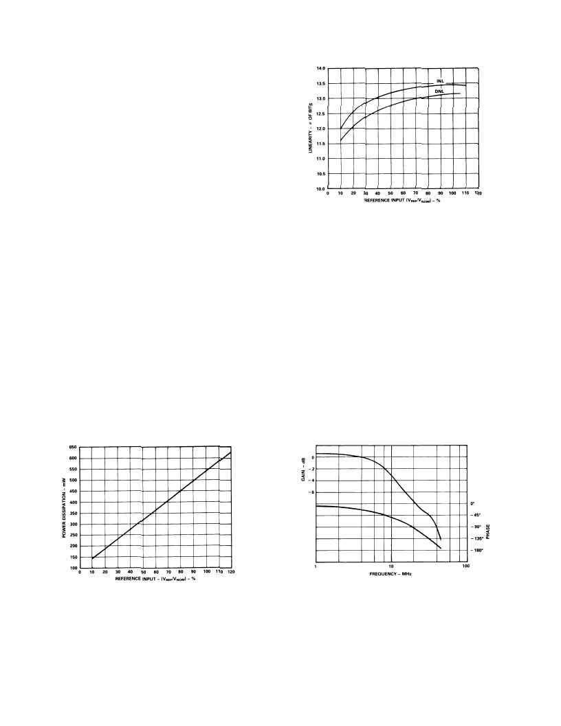
Power Consumption vs. V
REF
/V
NOM
As suggested in previous sections, most portions of AD668’s
current budget are proportional to the analog input signal. As a
result, operating the part at a reduced reference voltage offers
substantial power savings. This may be particularly attractive in
applications featuring a buffered output voltage, since the size of
the feedback resistor may be increased to compensate for the re-
duced DAC current. For example, the DAC could be config-
ured in the 5 V input mode, but driven with a 2.5 V reference,
producing a 5.12 mA full scale output. Reducing the output
level has performance ramifications in several areas, as demon-
strated later in this section, but the circuit designer is free to
trade power dissipation against performance to optimize the
AD668 for his application.
Figure 15. Power Consumption vs. Reference Level
Linearity vs. V
REF
/V
NOM
At reduced current levels, the linearity of the PNP DAC used in
the AD668 becomes more sensitive to the mismatch in transis-
tor V
BE
’s. As Figure 16 indicates, this effect starts to increase
fairly dramatically for reference levels less than 25% of nominal.
Increasing the current level above 100% does not appreciably
improve the linearity performance since the DAC has been
trimmed to perform optimally at the 100% reference level.
Figure 16. Linearity vs. Reference Level
AC PERFORMANCE
For the purposes of characterizing the frequency domain perfor-
mance of the AD668, all bits are turned on and the DAC is es-
sentially treated as a voltage amplifier/attenuator. The tests used
to generate these performance curves were done using the cir-
cuit shown in Figure 12.
AC characterization in the megahertz region is not trivial, and
special consideration is required to produce meaningful results.
Probe ground straps are inappropriate at these frequencies;
some type of probe socket is required. Signals should be routed
either on a PC board over a ground plane or through a coaxial
cable. Proper termination impedances should be used through-
out the fixturing.
Large Signal Frequency Response
Figure 17 represents the gain and phase response of a signal
swinging from 10% to 120% (peak to peak) of the nominal ref-
erence input. The DAC reference amplifier has an effective slew
rate or 30 V/
μ
s at the DAC output, so there will be slew-induced
distortion for full scale swings at greater than 10 MHz.
Figure 17. Large Signal Gain and Phase Response
Small Signal 3 dB Bandwidth vs. V
REF
/V
NOM
Figure 18 demonstrates the small signal (20% of nominal refer-
ence) bandwidth sensitivity to the analog input’s dc bias. The
small signal 3 dB bandwidth at 100% reference levels is greater
than 15 MHz, but the bandwidth remains greater than 10 MHz
over the entire nominal reference range. The differential gain
and phase for a 200 mV, 3 MHz signal are 0.5% and 2
°
,
respectively.
相關(guān)PDF資料 |
PDF描述 |
|---|---|
| AD668AQ | 12-Bit Ultrahigh Speed Multiplying D/A Converter |
| AD668J | 12-Bit Ultrahigh Speed Multiplying D/A Converter |
| AD668K | 12-Bit Ultrahigh Speed Multiplying D/A Converter |
| AD668KQ | RES 36.0 OHM 1/8W 1% 0805 SMD |
| AD668S | 12-Bit Ultrahigh Speed Multiplying D/A Converter |
相關(guān)代理商/技術(shù)參數(shù) |
參數(shù)描述 |
|---|---|
| AD668AQ | 制造商:Rochester Electronics LLC 功能描述:IC,MONO 12-BIT MULTI D/A - Bulk |
| AD668J | 制造商:AD 制造商全稱:Analog Devices 功能描述:12-Bit Ultrahigh Speed Multiplying D/A Converter |
| AD668JQ | 制造商:Analog Devices 功能描述:DAC 1-CH R-2R/Current Steering 12-bit 24-Pin CDIP Tube |
| AD668K | 制造商:AD 制造商全稱:Analog Devices 功能描述:12-Bit Ultrahigh Speed Multiplying D/A Converter |
| AD668KQ | 制造商:Analog Devices 功能描述: 制造商:Rochester Electronics LLC 功能描述: |
發(fā)布緊急采購,3分鐘左右您將得到回復(fù)。