- 您現(xiàn)在的位置:買賣IC網(wǎng) > PDF目錄8607 > AD8332ARUZ-RL (Analog Devices Inc)IC AMP VAR GAIN 2CHAN 28TSSOP PDF資料下載
參數(shù)資料
| 型號: | AD8332ARUZ-RL |
| 廠商: | Analog Devices Inc |
| 文件頁數(shù): | 1/56頁 |
| 文件大?。?/td> | 0K |
| 描述: | IC AMP VAR GAIN 2CHAN 28TSSOP |
| 標(biāo)準(zhǔn)包裝: | 2,500 |
| 系列: | X-AMP® |
| 類型: | 可變增益放大器 |
| 應(yīng)用: | 信號處理 |
| 安裝類型: | 表面貼裝 |
| 封裝/外殼: | 28-TSSOP(0.173",4.40mm 寬) |
| 供應(yīng)商設(shè)備封裝: | 28-TSSOP |
| 包裝: | 帶卷 (TR) |
| 配用: | AD8332-EVALZ-ND - BOARD EVAL FOR AD8332 |
當(dāng)前第1頁第2頁第3頁第4頁第5頁第6頁第7頁第8頁第9頁第10頁第11頁第12頁第13頁第14頁第15頁第16頁第17頁第18頁第19頁第20頁第21頁第22頁第23頁第24頁第25頁第26頁第27頁第28頁第29頁第30頁第31頁第32頁第33頁第34頁第35頁第36頁第37頁第38頁第39頁第40頁第41頁第42頁第43頁第44頁第45頁第46頁第47頁第48頁第49頁第50頁第51頁第52頁第53頁第54頁第55頁第56頁

Ultralow Noise VGAs with
Preamplifier and Programmable RIN
AD8331/AD8332/AD8334
Rev. G
Information furnished by Analog Devices is believed to be accurate and reliable. However, no
responsibilityis assumedbyAnalogDevicesforitsuse,norforanyinfringementsof patentsorother
rightsofthirdpartiesthatmayresultfromitsuse.Specificationssubjecttochangewithoutnotice.No
license is granted by implication or otherwise under any patent or patent rights of Analog Devices.
Trademarksandregisteredtrademarksarethepropertyoftheirrespectiveowners.
One Technology Way, P.O. Box 9106, Norwood, MA 02062-9106, U.S.A.
Tel: 781.329.4700
www.analog.com
Fax: 781.461.3113
2003–2010 Analog Devices, Inc. All rights reserved.
FEATURES
Ultralow noise preamplifier (preamp)
Voltage noise = 0.74 nV/√Hz
Current noise = 2.5 pA/√Hz
3 dB bandwidth
AD8331: 120 MHz
Low power
AD8331: 125 mW/channel
Wide gain range with programmable postamp
4.5 dB to +43.5 dB in LO gain mode
7.5 dB to 55.5 dB in HI gain mode
Low output-referred noise: 48 nV/√Hz typical
Active input impedance matching
Optimized for 10-bit/12-bit ADCs
Selectable output clamping level
Single 5 V supply operation
APPLICATIONS
Ultrasound and sonar time-gain controls
High performance automatic gain control (AGC) systems
I/Q signal processing
High speed, dual ADC drivers
GENERAL DESCRIPTION
channel, ultralow noise linear-in-dB, variable gain amplifiers
(VGAs). Optimized for ultrasound systems, they are usable as a
low noise variable gain element at frequencies up to 120 MHz.
Included in each channel are an ultralow noise preamp (LNA),
an X-AMP VGA with 48 dB of gain range, and a selectable gain
postamp with adjustable output limiting. The LNA gain is 19 dB
with a single-ended input and differential outputs. Using a single
resistor, the LNA input impedance can be adjusted to match a
signal source without compromising noise performance.
The 48 dB gain range of the VGA makes these devices suitable
for a variety of applications. Excellent bandwidth uniformity is
maintained across the entire range. The gain control interface
provides precise linear-in-dB scaling of 50 dB/V for control
voltages between 40 mV and 1 V. Factory trim ensures excellent
part-to-part and channel-to-channel gain matching.
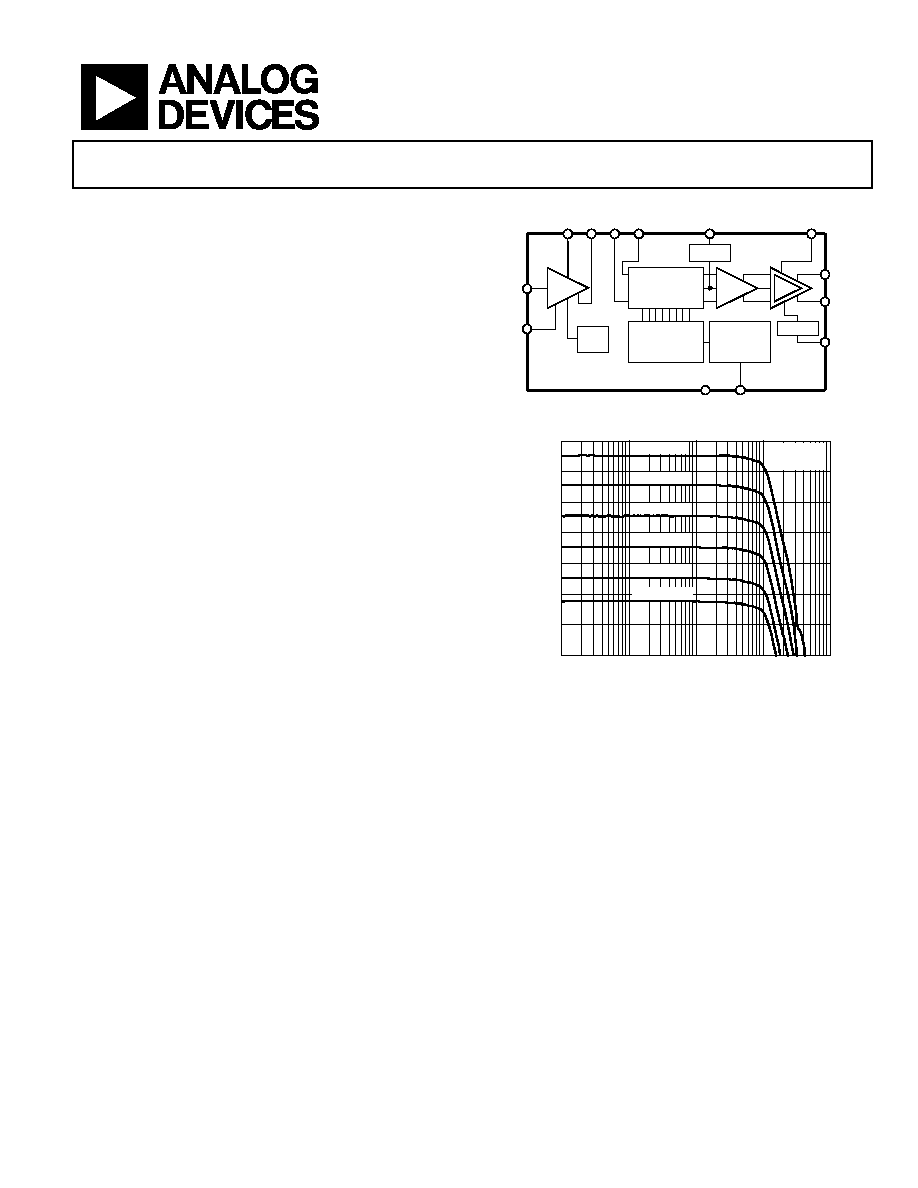
FUNCTIONAL BLOCK DIAGRAM
0
319
9-
0
01
VOL
VOH
VMID
LNA
48dB
ATTENUATOR
ENB
INH
LMD
VIN
VIP
LOP
LON
GAIN
AD8331/AD8332/AD8334
+
–
CLAMP
RCLMP
HILO
VCM
3.5dB OR 15.5dB
19dB
PA
VCM
BIAS
VGA BIAS AND
INTERPOLATOR
GAIN
CONTROL
INTERFACE
21dB
Figure 1. Signal Path Block Diagram
60
50
40
30
20
10
0
–10
100k
1M
10M
100M
1G
GA
IN
(
d
B
)
FREQUENCY (Hz)
03
19
9-
0
02
VGAIN = 1V
VGAIN = 0.8V
VGAIN = 0.6V
VGAIN = 0.4V
VGAIN = 0.2V
VGAIN = 0V
HI GAIN
MODE
Figure 2. Frequency Response vs. Gain
Differential signal paths result in superb second- and third-
order distortion performance and low crosstalk.
The low output-referred noise of the VGA is advantageous in
driving high speed differential ADCs. The gain of the postamp
can be pin selected to 3.5 dB or 15.5 dB to optimize gain range
and output noise for 12-bit or 10-bit converter applications. The
output can be limited to a user-selected clamping level, preventing
input overload to a subsequent ADC. An external resistor adjusts
the clamping level.
The operating temperature range is 40°C to +85°C. The
available in 28-lead TSSOP and 32-lead LFCSP packages, and
the AD8334 is available in a 64-lead LFCSP package.
相關(guān)PDF資料 |
PDF描述 |
|---|---|
| AD5328ARU | IC DAC 12BIT OCTAL W/BUF 16TSSOP |
| AD8332ACPZ-RL | IC AMP VAR GAIN 2CHAN 32LFCSP |
| SY88883VKG | IC POST AMP CML LP LIMIT 10-MSOP |
| VE-252-IV-F4 | CONVERTER MOD DC/DC 15V 150W |
| VE-22T-MY-B1 | CONVERTER MOD DC/DC 6.5V 50W |
相關(guān)代理商/技術(shù)參數(shù) |
參數(shù)描述 |
|---|---|
| AD8332-EVAL | 制造商:Analog Devices 功能描述:DUAL VGA - Bulk |
| AD8332-EVALZ | 功能描述:BOARD EVAL FOR AD8332 RoHS:是 類別:編程器,開發(fā)系統(tǒng) >> 評估板 - 運算放大器 系列:X-AMP® 產(chǎn)品培訓(xùn)模塊:Lead (SnPb) Finish for COTS Obsolescence Mitigation Program 標(biāo)準(zhǔn)包裝:1 系列:- |
| AD8333 | 制造商:AD 制造商全稱:Analog Devices 功能描述:DC to 50 MHz, Dual I/Q Demodulator and Phase Shifter |
| AD8333ACPZ | 制造商:Analog Devices 功能描述:I/Q DEMODULATOR DUAL LFCSP-32 制造商:Analog Devices 功能描述:I/Q, DEMODULATOR, DUAL, LFCSP-32 |
| AD8333ACPZ-REEL | 功能描述:IC DEMODULATOR DUAL I/Q 32LFCSP RoHS:是 類別:RF/IF 和 RFID >> RF 解調(diào)器 系列:- 產(chǎn)品培訓(xùn)模塊:Lead (SnPb) Finish for COTS Obsolescence Mitigation Program 標(biāo)準(zhǔn)包裝:2,500 系列:- 功能:解調(diào)器 LO 頻率:- RF 頻率:70MHz ~ 300MHz P1dB:-9dBm 增益:- 噪音數(shù)據(jù):6.36dB 電流 - 電源:41.5mA 電源電壓:2.7 V 封裝/外殼:28-WFQFN 裸露焊盤 供應(yīng)商設(shè)備封裝:28-TQFN-EP(5x5) 包裝:帶卷 (TR) |
發(fā)布緊急采購,3分鐘左右您將得到回復(fù)。