- 您現(xiàn)在的位置:買賣IC網(wǎng) > PDF目錄373968 > AD9801 (ANALOG DEVICES INC) CCD Signal Processor For Electronic Cameras(用于電子照相機(jī)的CCD信號(hào)處理器) PDF資料下載
參數(shù)資料
| 型號(hào): | AD9801 |
| 廠商: | ANALOG DEVICES INC |
| 元件分類: | 消費(fèi)家電 |
| 英文描述: | CCD Signal Processor For Electronic Cameras(用于電子照相機(jī)的CCD信號(hào)處理器) |
| 中文描述: | SPECIALTY CONSUMER CIRCUIT, PQFP48 |
| 封裝: | PLASTIC, TQFP-48 |
| 文件頁(yè)數(shù): | 9/12頁(yè) |
| 文件大小: | 265K |
| 代理商: | AD9801 |
AD9801
–9–
REV. 0
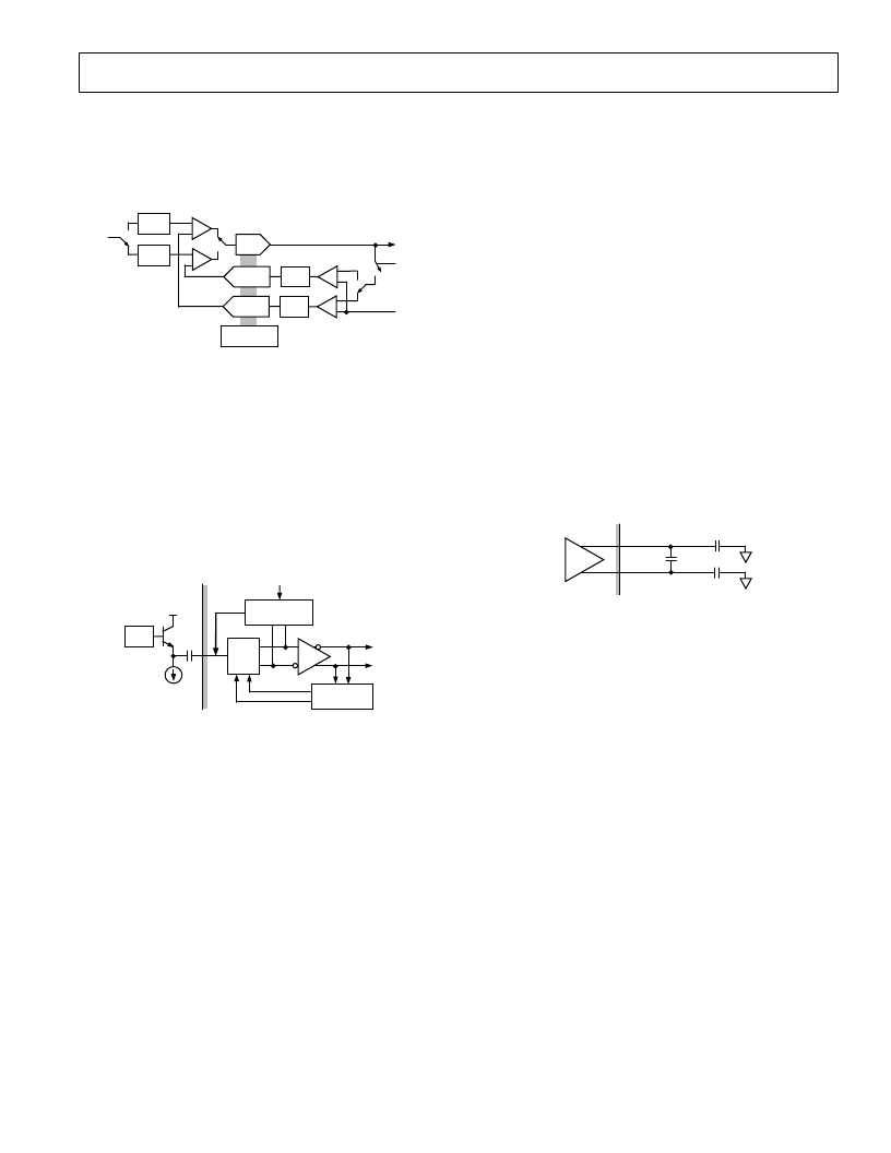
The actual implementation of this loop is slightly more compli-
cated as shown in Figure 18. Because there are two separate
CDS blocks, two black level feedback loops are required and
two offset voltages are developed. Figure 18 also shows an
additional PGA block in the feedback loop labeled “RPGA.”
PGA
ADC
IN
CLPOB
NEG REF
CONTROL
CDS1
RPGA2
INT2
CDS1
RPGA1
INT1
Figure 18.
The RPGA uses the same control inputs as the PGA, but has
the inverse gain. The RPGA functions to attenuate by the same
factor as the PGA amplifies, keeping the gain and bandwidth of
the loop constant.
Input Bias Level Clamping
The buffered CCD output is connected to the AD9801 through
an external coupling capacitor. The dc bias point for this coupling
capacitor is established during the clamping (CLPDM = LOW)
period using the “dummy clamp” loop shown in Figure 19.
When closed around the CDS, this loop establishes the desired
DC bias point on the coupling capacitor.
BLACK
LEVEL CLP
CCD
INPUT
CLAMP
CDS
CLPDM
TO ADC
PGA
Figure 19.
Input Blanking
In some applications, the AD9801’s input may be exposed to
large signals from the CCD. These signals can be very large,
relative to the AD9801’s input range, and could thus saturate
on-chip circuit blocks. Recovery time from such saturation
conditions could be substantial.
To avoid problems associated with processing these transients,
the AD9801 includes an input blanking function. When active
(PBLK = LOW), this function stops the CDS operation and
allows the user to disconnect the CDS inputs from the CCD
buffer.
If the input voltage exceeds the supply rail by more than
0.3 V, protection diodes will be turned on, increasing current
flow into the AD9801 (see Equivalent Input Circuits). Such
voltage levels should be externally clamped to prevent device
damage or reliability degradation.
10-Bit Analog-to-Digital Converter (ADC)
The ADC employs a multibit pipelined architecture, which is
well-suited for high throughput rates while being both area and
power efficient. The multistep pipeline presents a low input
capacitance resulting in lower on-chip drive requirements. A
fully differential implementation was used to overcome head-
room constraints of the single +3 V power supply.
Differential Reference
The AD9801 includes a 0.5 V reference based on a differential,
continuous-time bandgap cell. Use of an external bypass
capacitor reduces the reference drive requirements, thus
lowering the power dissipation. The differential architecture was
chosen for its ability to reject supply and substrate noise.
Recommended decoupling shown in Figure 20.
VRT
REF
VRB
1μF
0.1μF
0.1μF
Figure 20.
Internal Timing
The AD9801’s on-chip timing circuitry generates all clocks
necessary for operation of the CDS and ADC blocks. The user
needs only to synchronize the SHP and SHD clocks with the
CCD waveform, as all other timing is handled internally. The
ADCCLK signal is used to strobe the output data, and can be
adjusted to accommodate desired timing.
相關(guān)PDF資料 |
PDF描述 |
|---|---|
| AD9802JST | Silver Mica Capacitor; Capacitance:10pF; Capacitance Tolerance: 5%; Series:CD17; Voltage Rating:500VDC; Capacitor Dielectric Material:Mica; Termination:Radial Leaded; Lead Pitch:5.9mm; Leaded Process Compatible:Yes RoHS Compliant: Yes |
| AD9802 | .50" x 50 Black/Clear 240 Industrial Label Supply RoHS Compliant: NA |
| AD9803 | CCD And Video Signal Processor For Electronic Cameras(電子照相機(jī)的CCD信號(hào)和視頻信號(hào)處理器) |
| AD9805 | Complete 12-Bit/10-Bit 6 MSPS CCD/CIS Signal Processors |
| AD9805JS | Complete 12-Bit/10-Bit 6 MSPS CCD/CIS Signal Processors |
相關(guān)代理商/技術(shù)參數(shù) |
參數(shù)描述 |
|---|---|
| AD9801JCST | 制造商:Rochester Electronics LLC 功能描述:- Tape and Reel |
| AD9801JCSTRL | 制造商:Rochester Electronics LLC 功能描述:- Tape and Reel |
| AD9801JST | 制造商:Analog Devices 功能描述: |
| AD9802 | 制造商:AD 制造商全稱:Analog Devices 功能描述:CCD Signal Processor For Electronic Cameras |
| AD9802JST | 制造商:Rochester Electronics LLC 功能描述:- Bulk |
發(fā)布緊急采購(gòu),3分鐘左右您將得到回復(fù)。