- 您現(xiàn)在的位置:買賣IC網(wǎng) > PDF目錄378282 > ADC10838CIN (NATIONAL SEMICONDUCTOR CORP) 10-Bit Plus Sign Serial I/O A/D Converters with MUX, Sample/Hold and Reference PDF資料下載
參數(shù)資料
| 型號(hào): | ADC10838CIN |
| 廠商: | NATIONAL SEMICONDUCTOR CORP |
| 元件分類: | 模擬信號(hào)調(diào)理 |
| 英文描述: | 10-Bit Plus Sign Serial I/O A/D Converters with MUX, Sample/Hold and Reference |
| 中文描述: | SPECIALTY ANALOG CIRCUIT, PDIP24 |
| 封裝: | 0.600 INCH, PLASTIC, DIP-24 |
| 文件頁(yè)數(shù): | 7/30頁(yè) |
| 文件大?。?/td> | 453K |
| 代理商: | ADC10838CIN |
第1頁(yè)第2頁(yè)第3頁(yè)第4頁(yè)第5頁(yè)第6頁(yè)當(dāng)前第7頁(yè)第8頁(yè)第9頁(yè)第10頁(yè)第11頁(yè)第12頁(yè)第13頁(yè)第14頁(yè)第15頁(yè)第16頁(yè)第17頁(yè)第18頁(yè)第19頁(yè)第20頁(yè)第21頁(yè)第22頁(yè)第23頁(yè)第24頁(yè)第25頁(yè)第26頁(yè)第27頁(yè)第28頁(yè)第29頁(yè)第30頁(yè)
Electrical Characteristics
(Continued)
Note 1:
Absolute Maximum Ratings indicate limits beyond which damage to the device may occur.
Note 2:
Operating Ratings indicate conditions for which the device is functional, but do not guarantee specific performance limits. For guaranteed specifcations and
test conditions, see the Electrical Characteristics. The guaranteed specifications apply only for the test conditions listed. Some performance characteristics may
degrade when the device is not operated under the listed test conditions.
Note 3:
All voltages are measured with respect to GND, unless otherwise specified.
Note 4:
When the input voltage (V
IN
) at any pin exceeds the power supplies (V
IN
k
V
b
or V
IN
l
AV
a
or DV
a
), the current at that pln should be limited to 30 mA.
The 120 mA maximum package input current rating limits the number of pins that can safely exceed the power supplies with an input current of 30 mA to four.
Note 5:
The maximum power dissipation must be derated at elevated temperatures and is dictated by T
Jmax
,
i
JA
and the ambient temperature, T
A
. The maximum
allowable power dissipation at any temperature is P
D
e
(T
Jmax
b
T
A
)/
i
JA
or the number given In the Absolute Maximum Ratings, whichever is lower. For this
device, T
Jmax
e
150
§
C. The typical thermal resistance (
i
JA
) of these Paris when board mounted can be found in the following table:
Part Number
Thermal Resistance
Package Type
ADC10831CIN
82
§
C/W
90
§
C/W
47
§
C/W
80
§
C/W
47
§
C/W
80
§
C/W
60
§
C/W
75
§
C/W
N16E
ADC10831CIWM
M16B
ADC10832CIN
N20A
ADC10832CIWM
M20B
ADC10834CIN
N20A
ADC10834CIWM
M20B
ADC10838CIN
N24A
ADC10838CIWM
M24B
Note 6:
The human body model is a 100 pF capacitor discharged through a 1.5 k
X
resistor into each pin. The machine model is a 200 pF capacitor discharged
directly into each pin.
Note 7:
See AN-450 ‘‘Surface Mounting Methods and Their Effect on Product Reliability’’ or the section titied ‘‘Surtace Mount’’ found in any post 1986 National
Semiconductor Linear Data Book for other methods of soldering surtace mount devices.
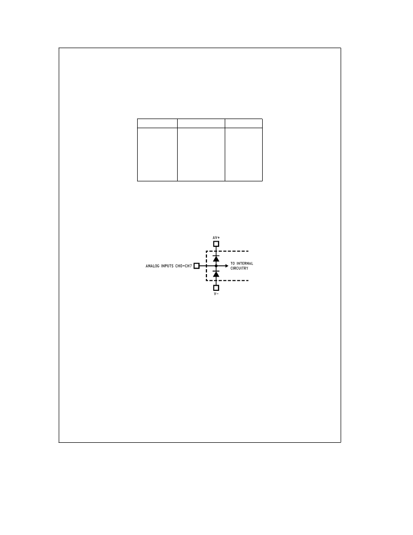
Note 8:
Two on-ohip diodes are tied to each analog input as shown below. They will forward-conduct for analog input voltages one diode drop below V
b
or one
diode drop greater than V
a
supply. Be careful during testing at low V
a
and V
b
levels (
g
4.5V), as high level analog inputs (
g
5V) can cause an input diode to
conduct, especially at elevated temperatures, which will cause errors In the conversion result. The specification allows 50 mV forward bias of either diode; this
means that as long as the analog V
IN
does not exceed the supply voltage by more than 50 mV, the output code will be oorrect. Exceeding this range on an
unselected channel will corrupt the reading of a selected channel. If AV
a
and DV
a
are minimum (4.5 V
DC
) and V
b
is a maximum (
b
4.5 V
DC
) full scale must be
sg
4.55 V
DC
.
TL/H/11391–6
Note 9:
No connection exists between AV
a
and DV
a
on the chip.
To guarantee accuracy, it is required that the AV
a
and DV
a
be connected together to a power supply with separate bypass filter at eacn V
a
pin.
Note 10:
One LSB is referenced to 10 bits of resolution.
Note 11:
Typicals are at T
J
e
T
A
e
25
§
C and represent most likely pararmetric norm.
Note 12:
Tested limits are guaranteed to National’s AOQL (Average Outgolng Quality Level).
Note 13:
Total unadjusted error includes offset, full-scale, linearity, multiplexer, and hold step errors.
Note 14:
The DC common-mode error is measured in the differential multiplexer mode with the assigned positive and negative input channels shorted together.
Note 15:
Channel leakage current is measured after the channel selection.
Note 16:
All the timing specifications are tested at the TTL logic levels, V
IL
e
0.8V for a falling edge and V
IH
e
2.0V for a rising. TRl-STATE voltage level is forced
to 1.4V.
Note 17:
The voltage applied to the digital inputs will affect the current drain during power down. These devices are tested with CMOS logic levels (logic Low
e
0V
and logic High
e
5V). TTL levels increase the power down current to about 300
m
A.
7
相關(guān)PDF資料 |
PDF描述 |
|---|---|
| ADC1173CIJM | 8-Bit, 3-Volt, 15MSPS, 33mW A/D Converter |
| ADC1173CIJMX | 8-Bit, 3-Volt, 15MSPS, 33mW A/D Converter |
| ADC1173 | 8-Bit, 3-Volt, 15MSPS, 33mW A/D Converter |
| ADC1173CIMTC | Pushbutton Switch; Switch Terminals:Solder Lug; Contact Current Max:5A; Leaded Process Compatible:Yes; Mounting Type:Panel; Switch Features:Lighted Indicator RoHS Compliant: Yes |
| ADC1173CIMTCX | Pushbutton Switch; Contact Current Max:5A; Contact Rating:5A; Leaded Process Compatible:Yes; Mounting Type:Panel; Size/Dimensions:HxWxD 0.708 x0.944 x1.65 in; Switch Features:Lighted Indicator |
相關(guān)代理商/技術(shù)參數(shù) |
參數(shù)描述 |
|---|---|
| ADC10838CIWM | 制造商:NSC 制造商全稱:National Semiconductor 功能描述:10-Bit Plus Sign Serial I/O A/D Converters with MUX, Sample/Hold and Reference |
| ADC108S022 | 制造商:NSC 制造商全稱:National Semiconductor 功能描述:8-Channel, 50 kSPS to 200 kSPS, 10-Bit A/D Converter |
| ADC108S022CIMT | 功能描述:模數(shù)轉(zhuǎn)換器 - ADC RoHS:否 制造商:Texas Instruments 通道數(shù)量:2 結(jié)構(gòu):Sigma-Delta 轉(zhuǎn)換速率:125 SPs to 8 KSPs 分辨率:24 bit 輸入類型:Differential 信噪比:107 dB 接口類型:SPI 工作電源電壓:1.7 V to 3.6 V, 2.7 V to 5.25 V 最大工作溫度:+ 85 C 安裝風(fēng)格:SMD/SMT 封裝 / 箱體:VQFN-32 |
| ADC108S022CIMT/NOPB | 功能描述:模數(shù)轉(zhuǎn)換器 - ADC 8CH,50KSPS-200KSPS, 10B ADC RoHS:否 制造商:Texas Instruments 通道數(shù)量:2 結(jié)構(gòu):Sigma-Delta 轉(zhuǎn)換速率:125 SPs to 8 KSPs 分辨率:24 bit 輸入類型:Differential 信噪比:107 dB 接口類型:SPI 工作電源電壓:1.7 V to 3.6 V, 2.7 V to 5.25 V 最大工作溫度:+ 85 C 安裝風(fēng)格:SMD/SMT 封裝 / 箱體:VQFN-32 |
| ADC108S022CIMTX | 功能描述:模數(shù)轉(zhuǎn)換器 - ADC RoHS:否 制造商:Texas Instruments 通道數(shù)量:2 結(jié)構(gòu):Sigma-Delta 轉(zhuǎn)換速率:125 SPs to 8 KSPs 分辨率:24 bit 輸入類型:Differential 信噪比:107 dB 接口類型:SPI 工作電源電壓:1.7 V to 3.6 V, 2.7 V to 5.25 V 最大工作溫度:+ 85 C 安裝風(fēng)格:SMD/SMT 封裝 / 箱體:VQFN-32 |
發(fā)布緊急采購(gòu),3分鐘左右您將得到回復(fù)。