- 您現(xiàn)在的位置:買賣IC網(wǎng) > PDF目錄378283 > ADC12048 (National Semiconductor Corporation) 12-Bit Plus Sign 216 kHz 8-Channel Sampling Analog-to-Digital Converter PDF資料下載
參數(shù)資料
| 型號: | ADC12048 |
| 廠商: | National Semiconductor Corporation |
| 英文描述: | 12-Bit Plus Sign 216 kHz 8-Channel Sampling Analog-to-Digital Converter |
| 中文描述: | 12位帶符號216 kHz的8聲道采樣模擬到數(shù)字轉(zhuǎn)換器 |
| 文件頁數(shù): | 22/30頁 |
| 文件大?。?/td> | 635K |
| 代理商: | ADC12048 |
第1頁第2頁第3頁第4頁第5頁第6頁第7頁第8頁第9頁第10頁第11頁第12頁第13頁第14頁第15頁第16頁第17頁第18頁第19頁第20頁第21頁當(dāng)前第22頁第23頁第24頁第25頁第26頁第27頁第28頁第29頁第30頁
Register Bit Description
(Continued)
b
11
b
10
b
9
0
1
Command
0
0
0
0
Standby command. This puts the ADC in a low power consumption mode
Ful-Cal command. This will cause the ADC to perform a self-calibrating cycle that will correct
linearity and zero errors.
Auto-zero command. This will cause the ADC to perform an auto-zero cycle that corrects
offset errors.
Reset command. This puts the ADC in an idle mode.
Start command. This will put the converter in a start mode, preparing it to perform a
conversion. If in asynchronous mode (b
8
= “0”), conversions will immediately begin after the
programmed acquisition time has ended. In synchronous mode (b
8
= “1”), conversions will
begin after a rising edge appears on the SYNC pin.
0
1
0
0
1
1
0
1
0
b
12
:
This is the Bus Width (BW) bit. When this bit is a ’0’ the ADC12048 is configured to interface with an 8-bit data bus; data pins
D
–D
are active and pins D
–D
9
are in TRI-STATE. When the BW bit is a ’1’, the ADC12048 is configured to interface with a
16-bit data bus and data pins D
13
–D
0
are all active. The BW bit is a ’0’ at
power-up.
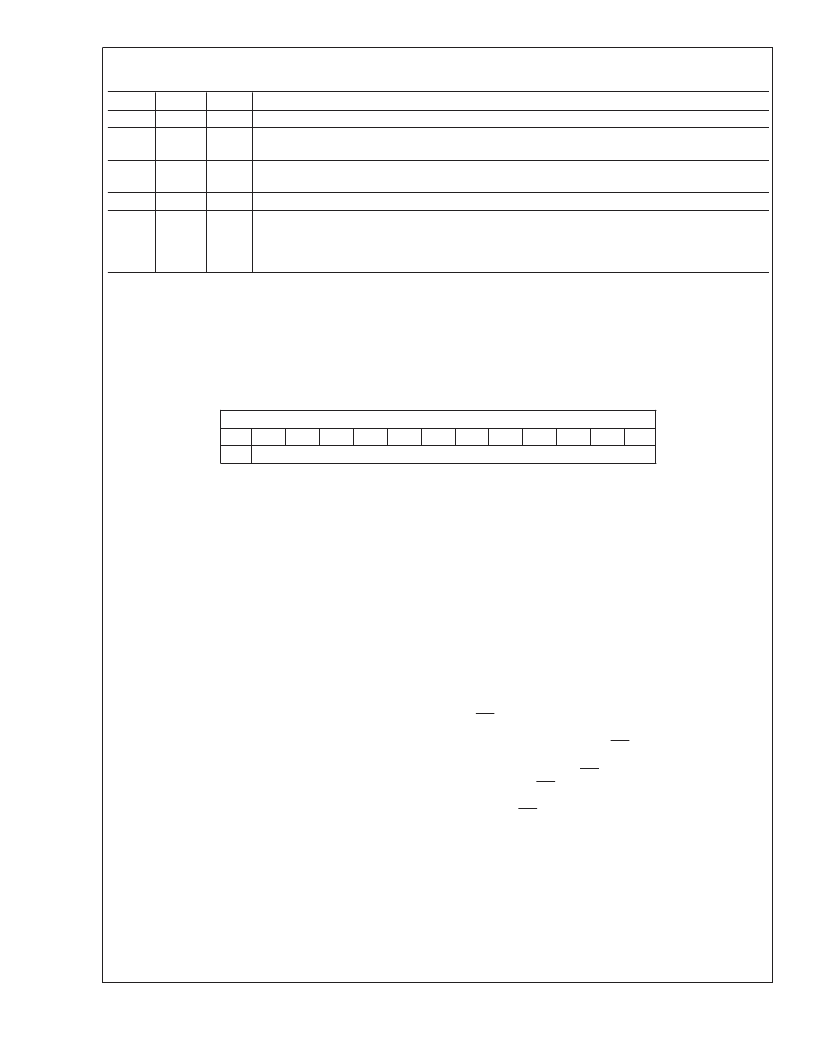
DATA REGISTER (Read Only)
This is a 13-bit read only register that holds the 12-bit +sign conversion result in two’s compliment form. All reads performed from
the ADC12048 will place the contents of this register on the data bus. When reading the data register in 8-bit mode, the sign bit
is extended (b
12
through b
8
all contain the sign bit).
MSB
b
12
sign
LSB
b
0
b
11
b
10
b
9
b
8
b
7
b
6
b
5
b
4
b
3
b
2
b
1
Conversion Data
Power on State:
0000Hex
b
11
–b
0
:
b
11
is the most significant bit and b
0
is the least significant bit of the conversion result.
b
12
:
This bit contains the sign of the conversion result: 0 for positive results and 1 for negative.
Functional Description
The ADC12048 is programmed through a digital interface
that supports an 8-bit or 16-bit data bus. The digital interface
consists of a 13-bit data input/output bus (D
12
–D
0
), digital
control signals and two internal registers: a
write
only 13-bit
Configuration
register and a
read
only 13-bit
Data
register.
The Configuration register programs the functionality of the
ADC12048. The 13 bits of the Configuration register are di-
vided into 7 fields. Each field controls a specific function of
the ADC12048: the channel selection of the MUX, the acqui-
sition time, synchronous or asynchronous conversions,
mode of operation and the data bus size.
Features and Operating Modes
SELECTABLE BUS WIDTH
TheADC12048 can be programmed to interface with an 8-bit
or 16-bit data bus. The BW bit (b
) in the Configuration reg-
ister controls the bus size. The bus width is set to
8 bits
(D
–D
are active and D
–D
are in TRI-STATE) if the BW
bit is cleared or
13 bits
(D
–D
are active) if the BW bit is
set. At
power-up
the bus width defaults to 8 bits and any ini-
tial programming of the ADC12048 should take this into con-
sideration.
In
8-bit
mode the Configuration register is byte accessible.
The HB bit in the lower byte of the Configuration register is
used to access the upper byte. If the HB bit is set with a write
to the lower byte, the next byte written to the ADC will be
placed in the upper byte of the Configuration register. After
data is written to the upper byte of the Configuration register,
the HB bit will automatically be cleared, causing the next
byte written to the ADC to go to the lower byte of the Con-
figuration register. When reading the ADC in 8-bit mode, the
first read cycle places the lower byte of the Data register on
the data bus followed by the upper byte during the next read
cycle.
In
13-bit
mode the HB bit is a don’t care condition and all bits
of the data register and Configuration register are accessible
with a single read or write cycle. Since the bus width of the
ADC12048 defaults to 8 bits after power-up, the first action
when 13-bit mode is desired must be set to the bus width to
13 bits.
WMODE
The WMODE pin is used to determine the active edge of the
write pulse. The state of this pin determines which edge of
the WR signal will cause theADC to latch in data. This is pro-
cessor dependent. If the processor has valid data on the bus
during the falling edge of the WR signal, the WMODE pin
must be tied to V
+. This will cause theADC to latch the data
on the falling edge of the WR signal. If data is valid on the ris-
ing edge of the WR signal, the WMODE pin must be tied to
DGND causing the ADC to latch in the data on the rising
edge of the WR signal.
INPUT MULTIPLEXER
The ADC12048 has an eight channel input multiplexer with a
COM
input
that
can
be
pseudo-differential or fully-differential mode. The MUX select
bits (b
–b
) in the Configuration register determine which
channels will appear at the MUXOUT+ and MUXOUT mul-
tiplexer output pins. (Refer to Register Bit Description Sec-
tion.) Analog signal conditioning with fixed-gain amplifiers,
programmable-gain amplifiers, filters and other processing
circuits can be used at the output of the multiplexer before
used
in
a
single-ended,
A
www.national.com
22
相關(guān)PDF資料 |
PDF描述 |
|---|---|
| ADC12048CIV | 12-Bit Plus Sign 216 kHz 8-Channel Sampling Analog-to-Digital Converter |
| ADC1205CCJ-1 | 12-Bit Plus Sign mP Compatible A/D Converters |
| ADC1225 | 12-Bit Plus Sign mP Compatible A/D Converters |
| ADC1205 | 12-Bit Plus Sign mP Compatible A/D Converters |
| ADC1205CCJ | NiCd/NiMH Gas Gauge W/1-Wire (DQ) I/F, 5 LED Drivers, Control Signals For BQ2004 Fast-Charge IC 16-SOIC 0 to 70 |
相關(guān)代理商/技術(shù)參數(shù) |
參數(shù)描述 |
|---|---|
| ADC12048_02 | 制造商:NSC 制造商全稱:National Semiconductor 功能描述:12-Bit Plus Sign 216kHz 8-Channel Sampling Analog-to-Digital Converter |
| ADC12048CIV | 功能描述:模數(shù)轉(zhuǎn)換器 - ADC RoHS:否 制造商:Texas Instruments 通道數(shù)量:2 結(jié)構(gòu):Sigma-Delta 轉(zhuǎn)換速率:125 SPs to 8 KSPs 分辨率:24 bit 輸入類型:Differential 信噪比:107 dB 接口類型:SPI 工作電源電壓:1.7 V to 3.6 V, 2.7 V to 5.25 V 最大工作溫度:+ 85 C 安裝風(fēng)格:SMD/SMT 封裝 / 箱體:VQFN-32 |
| ADC12048CIV/NOPB | 功能描述:模數(shù)轉(zhuǎn)換器 - ADC RoHS:否 制造商:Texas Instruments 通道數(shù)量:2 結(jié)構(gòu):Sigma-Delta 轉(zhuǎn)換速率:125 SPs to 8 KSPs 分辨率:24 bit 輸入類型:Differential 信噪比:107 dB 接口類型:SPI 工作電源電壓:1.7 V to 3.6 V, 2.7 V to 5.25 V 最大工作溫度:+ 85 C 安裝風(fēng)格:SMD/SMT 封裝 / 箱體:VQFN-32 |
| ADC12048CIVF | 功能描述:模數(shù)轉(zhuǎn)換器 - ADC RoHS:否 制造商:Texas Instruments 通道數(shù)量:2 結(jié)構(gòu):Sigma-Delta 轉(zhuǎn)換速率:125 SPs to 8 KSPs 分辨率:24 bit 輸入類型:Differential 信噪比:107 dB 接口類型:SPI 工作電源電壓:1.7 V to 3.6 V, 2.7 V to 5.25 V 最大工作溫度:+ 85 C 安裝風(fēng)格:SMD/SMT 封裝 / 箱體:VQFN-32 |
| ADC12048CIVF/NOPB | 功能描述:模數(shù)轉(zhuǎn)換器 - ADC 12B PLUS SIGN 216KHz 8CH SAMPLING ADC RoHS:否 制造商:Texas Instruments 通道數(shù)量:2 結(jié)構(gòu):Sigma-Delta 轉(zhuǎn)換速率:125 SPs to 8 KSPs 分辨率:24 bit 輸入類型:Differential 信噪比:107 dB 接口類型:SPI 工作電源電壓:1.7 V to 3.6 V, 2.7 V to 5.25 V 最大工作溫度:+ 85 C 安裝風(fēng)格:SMD/SMT 封裝 / 箱體:VQFN-32 |
發(fā)布緊急采購,3分鐘左右您將得到回復(fù)。